Semiconductor device with ground shielding structure

一种接地屏蔽、半导体的技术,应用在具有接地屏蔽结构的半导体器件领域,能够解决大涡流损耗、电感Q值下降、连接面积大等问题,达到降低涡流损耗、避免Q值的效果

Active Publication Date: 2014-05-14
SEMICON MFG INT (SHANGHAI) CORP
View PDF6 Cites 7 Cited by
  • Summary
  • Abstract
  • Description
  • Claims
  • Application Information

AI Technical Summary

Problems solved by technology

However, the patterned structure will form a larger coupling capacitance at high frequencies, and the middle area of ​​the shielding structure will have a larger connection area, which will generate a larger eddy current loss, resulting in a decrease in the Q value of the inductor

Method used


Image

  • Semiconductor device with ground shielding structure
  • Semiconductor device with ground shielding structure
  • Semiconductor device with ground shielding structure

Examples


no. 1 example

[0045] Please refer to figure 2 , is a top view of the ground shielding structure and the ground ring described in this embodiment, wherein the substrate, the isolation structure, and the dielectric layer are not shown.

[0046] The ground shielding structure provided in this embodiment is composed of the first active area ring 120 and the metal wire 140 on the surface of the substrate, and the ground shielding structure is grounded through the ground ring 110 .

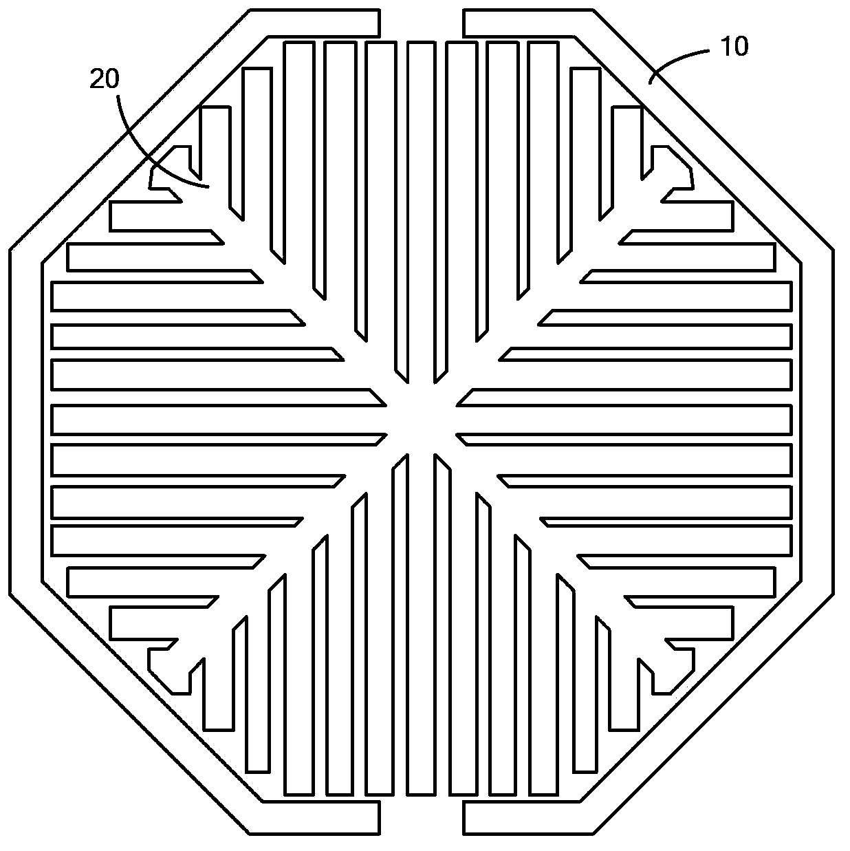
[0047] Specifically, the active area ring 120 is located on the surface of the substrate. In this embodiment, there are eight active area rings 120. In other embodiments of the present invention, the number of the active area rings may be Any number from 2 to 100, such as 10, 20 or 50. The active area ring 120 is octagonal in shape.

[0048] The ground ring 110 is located outside the active area ring 120 and surrounds the active area ring 120 , and the ground ring 110 is octagonal. In other embodiments of the pre...

no. 2 example

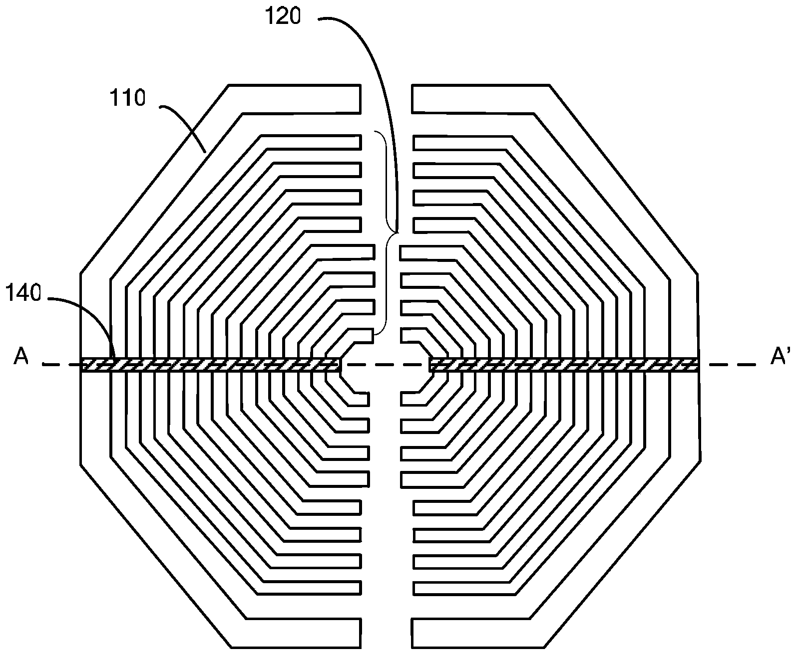
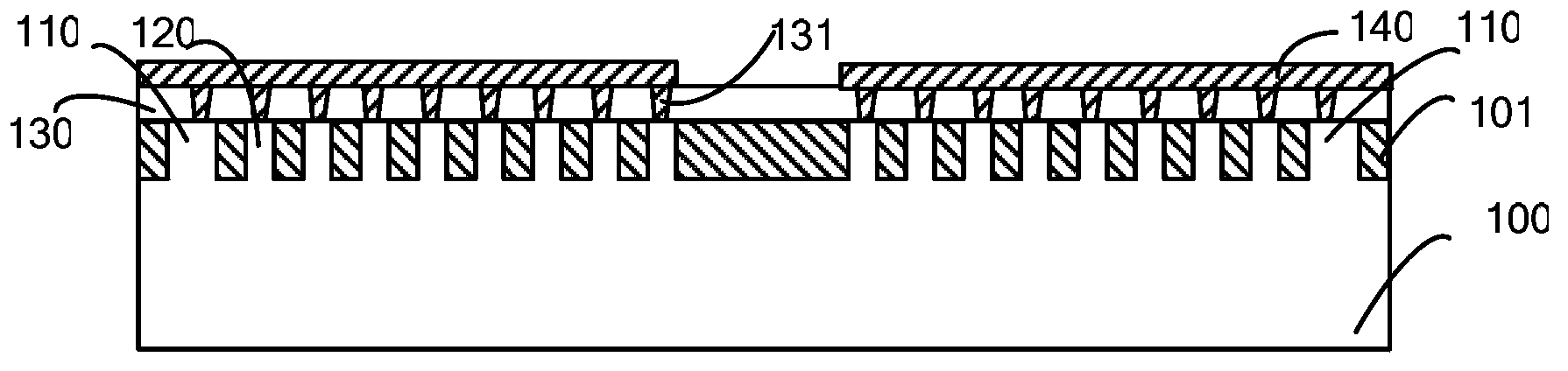
[0053] Please refer to Figure 4 , Figure 5 , Image 6 and Figure 7 , Figure 4 It is a schematic cross-sectional view of a ground shielding structure and a ground ring according to the second embodiment of the present invention; Figure 5 is a top view of the first active area ring 220 of the ground shield structure and the second active area ring 210 of the ground ring; Image 6 It is a top view of the polysilicon ring of the ground shielding structure in this embodiment; Figure 7 It is a top view of the first metal ring 420 of the ground shielding structure, the second metal ring 410 of the ground ring and the metal wire 440 of the present embodiment.

[0054] figure 1 , which is a schematic cross-sectional view of the ground shielding structure in the direction AA'. The ground shielding structure of this embodiment includes: a first active region ring 220, a polysilicon ring 320 and a first metal ring 420 (please refer to Figure 7 ) and wire 440 (please refer t...


PUM

PropertyMeasurementUnit
widthaaaaaaaaaa

Abstract

Provided is a semiconductor device with a ground shielding structure. The ground shielding structure comprises a substrate, a ground ring on the surface of the substrate, and a ground shielding structure arranged on the surface of the substrate and surrounded by the ground ring, wherein the ground shielding structure comprises multiple coaxial conducting rings, a metal line passing through the multiple conducting rings along the radius directions of the conducting rings and electrically connected with the ground ring, an insulating layer between the ground shielding structure and the an electronic device, and an electronic device on the insulating layer. The ground shielding structure may effectively decrease the substrate loss of the electronic device.

Description

technical field [0001] The invention relates to the technical field of semiconductors, in particular to a semiconductor device with a ground shielding structure. Background technique [0002] In an existing integrated circuit, such as a CMOS radio frequency integrated circuit, an inductor is an important electrical device, and its performance parameters directly affect the performance of the integrated circuit. In the prior art, planar inductors are mostly used as inductors in integrated circuits, such as planar spiral inductors. The planar inductor is formed by winding metal wires on the surface of the substrate or dielectric layer. Compared with the traditional wire wound inductor, the planar inductor has the advantages of low cost, easy integration, low noise and low power consumption. More importantly, it can Compatible with today's IC processes. The quality factor Q of the inductor is the ratio of the energy stored in the inductor to the energy lost in each oscillatio...

Claims


Application Information

Patent Timeline
Patent Type & Authority Applications(China)
IPC IPC(8): H01L23/522H01F17/00
CPCH01L23/5225H01L2924/0002H01L23/5227H01L23/552H01L28/10H01L2223/6655H01L23/66H01L2924/00
Inventor 程仁豪王西宁刘凌
Owner SEMICON MFG INT (SHANGHAI) CORP
Why Eureka
Try Eureka