
Anti-irradiation Technology and Implementation Method Based on Back Gate Transistor

An anti-radiation, transistor technology, applied in the direction of electric solid-state devices, semiconductor devices, semiconductor/solid-state device components, etc., can solve the problems of integration limitations, application limitations, and high costs, and achieve improved performance, low cost, and high speed. Effect

Active Publication Date: 2017-01-11
SHANGHAI XINCHU INTEGRATED CIRCUIT
View PDF5 Cites 0 Cited by
  • Summary
  • Abstract
  • Description
  • Claims
  • Application Information

AI Technical Summary

Problems solved by technology

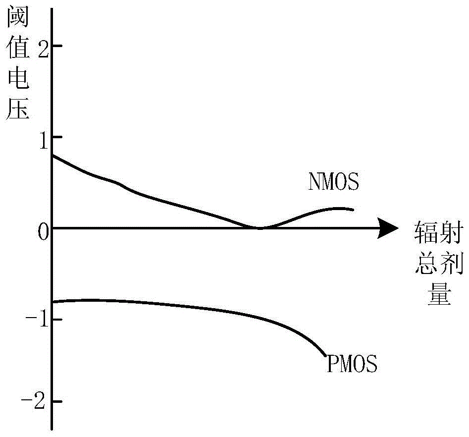
Some advanced anti-radiation technologies, such as the technology of CMOS / SOS technology laboratory to epitaxially manufacture CMOS devices on synthetic sapphire insulating substrates, have successfully solved the problem of dielectric isolation and have strong anti-radiation capabilities, but there are major problems in SOS reinforcement. Both are material dependent and integration is limited due to the effect of stress between silicon and sapphire
GaAs radiation-resistant devices have also received special attention due to their high-speed, high-frequency, high-power, and extremely high radiation-resistant capabilities. limit

Method used


Image

  • Anti-irradiation Technology and Implementation Method Based on Back Gate Transistor
  • Anti-irradiation Technology and Implementation Method Based on Back Gate Transistor
  • Anti-irradiation Technology and Implementation Method Based on Back Gate Transistor

Examples


Embodiment Construction

[0037] The specific embodiment of the present invention will be further described below in conjunction with accompanying drawing:

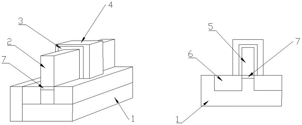
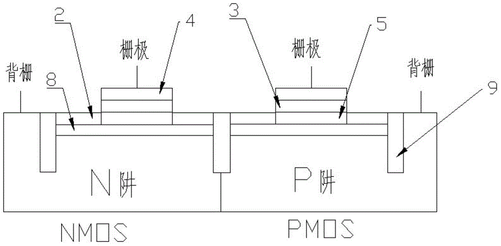
[0038] The anti-irradiation technology proposed in the present invention is based on a transistor structure with a back gate bias, which can be a bulk silicon transistor or a silicon-on-insulator (SOI) transistor; it can be a general MOS transistor or a Emerging Finfet transistors. A bulk silicon Finfet structure with back gate bias such as figure 2As shown, 1 is the substrate, which is also the back gate bias layer of the transistor, 2 is the doped source region or drain region, 3 is the gate oxide layer, 4 is the gate of the transistor, and 5 is the Fin of the transistor. The channel, 6 is an insulating structure, and 7 is an insulating oxide layer, which also constitutes the oxide layer of the back gate. An insulating structure 6 is embedded on the back gate bias layer 1, and an insulating oxide layer 7 is covered on the surface of the back ...


PUM


Abstract

The invention relates to a back gate transistor-based anti-radiation technology and an implementation method of the technology. The technology comprises the steps of firstly, inputting a boundary scan test signal, and detecting an output signal; comparing the detected output signal with an ideal output signal, if the detected output signal is approximate to the ideal output signal, stopping testing, and if the detected output signal is more different from the ideal output signal, changing the back gate bias of all blocks in a chip by building a built-in self-optimizer; adjusting the threshold voltage of transistors in all the blocks, and then detecting the output signal; and repeating the operation until the detected output signal is approximate to the ideal output signal to the utmost extent. The boundary scan test is used for detecting, and the back gate bias can be adjusted by the built-in self-optimizer, so that the threshold voltage offset of the transistors can be effectively inhibited, the performances of the transistors can be improved, and the function of radiation resistance can be reached; and furthermore, the anti-radiation technology has the characteristics of being high in integration level, rapid in speed, high in radiation resistance and the like, and is low in cost, simple in technology and easy to implement.

Description

technical field [0001] The invention relates to the field of semiconductor manufacturing, in particular to a back-gate transistor-based anti-radiation technology and an implementation method. Background technique [0002] The development and application of military microelectronics technology has greatly promoted the development of military equipment and weapon systems, and greatly improved the adaptability and combat capability of military equipment and weapon systems. In order to enable military electronic systems to work stably in harsh environments such as nuclear explosions, space radiation, and nuclear power, it is necessary to conduct radiation-resistant hardening research on basic components and integrated circuits. Especially since the United States began to implement the Star Wars (Strategic Defense) program in 1983, the research on the anti-radiation hardening technology of integrated circuits has been highly valued. The development of microelectronic technology ...

Claims


Application Information

Patent Timeline
Patent Type & Authority Patents(China)
IPC IPC(8): H01L27/04H01L23/552H01L21/66
CPCH01L2924/0002
Inventor 亢勇陈邦明
Owner SHANGHAI XINCHU INTEGRATED CIRCUIT
Learn More