Inverted top emission organic electroluminescence device and preparation method thereof

A luminescence and top emission technology, applied in the field of electric light sources, can solve the problems of inconvenient heat supply and speed adjustment, uneven structure of the transport doped layer, and influence on carrier injection efficiency, etc., so as to improve electron transport efficiency and luminescence Efficiency, the effect of improving uniform performance and stable performance

Active Publication Date: 2014-06-11
OCEANS KING LIGHTING SCI&TECH CO LTD +2
View PDF7 Cites 8 Cited by
  • Summary
  • Abstract
  • Description
  • Claims
  • Application Information

AI Technical Summary

Problems solved by technology

However, for dopants and matrix materials with a large difference in melting point, such as when inorganic dopants and organic matrix materials are used, the heat supply and speed adjustment during the co-doping process are inconvenient due to the large difference in melting point. , leading to the inhomogeneous structure of the obtained transport doped layer, resulting in unstable performance, which affects the carrier injection efficiency

Method used


Image

  • Inverted top emission organic electroluminescence device and preparation method thereof
  • Inverted top emission organic electroluminescence device and preparation method thereof
  • Inverted top emission organic electroluminescence device and preparation method thereof

Examples


preparation example Construction

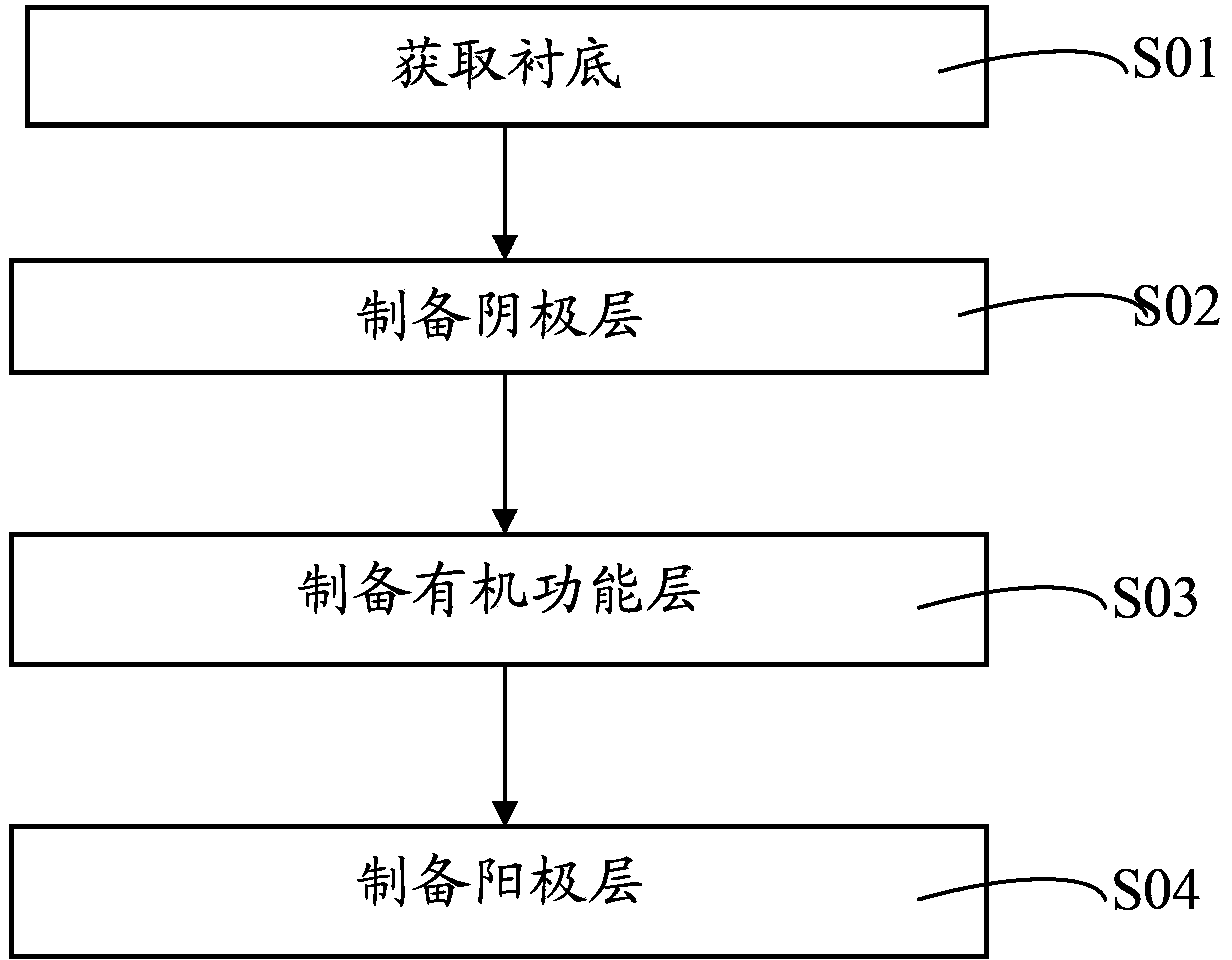
[0032] Correspondingly, an embodiment of the present invention also provides a method for manufacturing the above-mentioned inverted top emission organic electroluminescence device. The process of the preparation method is as follows image 3 shown, see also figure 1 , 2 , including the following steps:

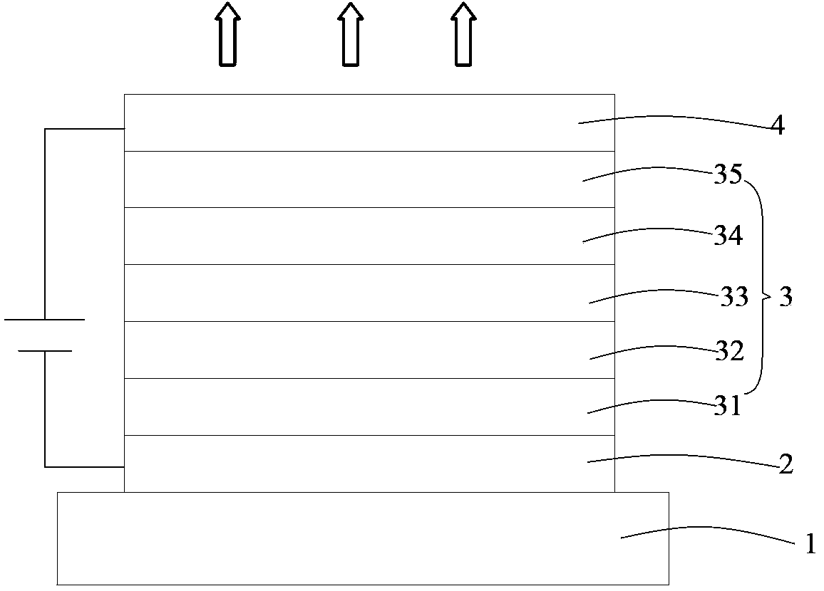
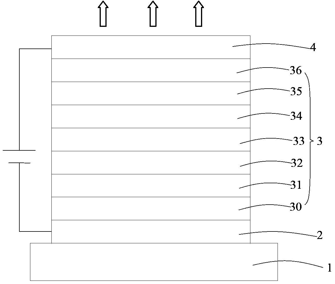
[0033] S01. Obtain the substrate: obtain the substrate of the required size according to actual needs as the substrate layer 1;

[0034] S02. Prepare the cathode layer 2: plate the cathode layer 2 on one surface of the substrate layer 1;

[0035] S03. Prepare the organic functional layer 3: the surface of the cathode layer 2 prepared in step S02 opposite to the substrate layer 1 is coated with an organic functional layer 3, wherein the organic functional layer 3 includes an electron transport layer 31 and is driven by an external power supply. The light-emitting layer 33 that emits light from the bottom, and the electron transport layer 31 is stacked and combined between ...

Embodiment 1

[0061] An organic electroluminescent device with inverted top emission, its structure is glass substrate / Al(70nm) / electron transport layer / TPBi(10nm) / DPVBi(20nm) / TPD(10nm) / F4-TCNQ:MeO-TPD (25nm) / Al(18nm); wherein the precursor structure of the electron transport layer is LiF(0.5nm) / TPBi(10nm) / LiF(0.5nm) / TPBi(10nm), the electron transport layer is composed of the electron transport layer The precursor is obtained through the following heat treatment in Example 1.

[0062] The preparation method of the inverted top emission organic electroluminescence device comprises the following steps:

[0063] Step S11. Provide a glass substrate: place the glass substrate in deionized water containing detergent for ultrasonic cleaning, and after cleaning, use isopropanol and acetone in ultrasonic treatment for 20 minutes, and then dry it with nitrogen for use;

[0064] Step S12. At a vacuum degree of 5×10 -4 In the coating system of Pa, the Al cathode layer is prepared on the glass substra...

Embodiment 2

[0075] An organic electroluminescent device with inverted top emission, its structure is glass substrate / Ag(100nm) / electron transport layer / TPBi(10nm) / DPVBi(20nm) / TPD(10nm) / F4-TCNQ:CuPc(25nm ) / Ag(20nm); the precursor structure of the electron transport layer is Li 2 CO 3 (1nm) / Alq 3 (9nm) / Li 2 CO 3 (1nm) / Alq 3 (9nm), the electron transport layer is formed by the electron transport layer precursor through the following heat treatment in Example 1.

[0076] The preparation method of the inverted top emission organic electroluminescence device comprises the following steps:

[0077] Step S21. Provide a glass substrate: perform cleaning treatment with reference to the treatment method in Example 1;

[0078] Step S22. When the degree of vacuum is 5×10 -4 In the coating system of Pa, the Ag cathode layer is prepared on the glass substrate in step S21, and the evaporation speed of the Ag cathode layer is 0.5nm / s;

[0079] Step S23. When the degree of vacuum is 5×10 -4 In the...


PUM


Abstract

The invention discloses an inverted top emission organic electroluminescence device and a preparation method thereof. The inverted top emission organic electroluminescence device comprises a substrate layer, a cathode layer, an organic functional layer and an anode layer which are laminated and combined in turn. The organic functional layer comprises an electron transmission layer and a light-emitting layer which emits light under driving of an external power supply. The electron transmission layer is arranged between the cathode layer and the light-emitting layer in a laminating and combining way. The electron transmission layer has a structure of a doped layer which is formed by multiple doping agent layers and electron transmission matrix material layers in an alternating and laminating way after permeating and doping processing. The preparation method of the inverted top emission organic electroluminescence device comprises steps that: a substrate is acquired, the cathode layer is prepared, the organic functional layer is prepared, the anode layer is prepared, etc. The inverted top emission organic electroluminescence device is high in light emission efficiency, low in starting voltage and long in the service life. The preparation method of the inverted top emission organic electroluminescence device is simple in technology, conditions are easy to control and product qualified rate is high so that production efficiency is effectively enhanced and the inverted top emission organic electroluminescence device is suitable for industrialized production.

Description

technical field [0001] The invention belongs to the technical field of electric light sources, and in particular relates to an organic electroluminescent device with inverted top emission and a preparation method thereof. Background technique [0002] Organic Light Emission Diode (hereinafter referred to as OLED) has the characteristics of high brightness, wide range of material selection, low driving voltage, full-cured active light emission, etc., and has the advantages of high definition, wide viewing angle, and fast response speed. A display technology and light source with great potential, in line with the development trend of mobile communication and information display in the information age, and the requirements of green lighting technology, is the focus of many researchers at home and abroad. [0003] So far, although researchers from all over the world have greatly improved the performance indicators of the device by selecting suitable organic materials and reasona...

Claims


Application Information

Patent Timeline
Patent Type & Authority Applications(China)
IPC IPC(8): H01L51/50H01L51/56
CPCH10K50/165H10K50/167
Inventor 周明杰王平冯小明张振华
Owner OCEANS KING LIGHTING SCI&TECH CO LTD
Why Eureka
Try Eureka