Manufacturing method of submicron photonic crystal phase array light beam splitter

A production method and technology of photonic crystals, applied in optics, instruments, optical components, etc., can solve problems such as crystal structure complexity, achieve uniform intensity distribution, and expand the application range

Inactive Publication Date: 2014-06-25
BEIJING JIAOTONG UNIV
View PDF4 Cites 6 Cited by
  • Summary
  • Abstract
  • Description
  • Claims
  • Application Information

AI Technical Summary

Problems solved by technology

This unique periodic photonic microstructure has a wide range of applications in many fields, especially in 1998 Berger proposed the concept of a two-dimensional periodically polarized photonic microstructure crystal, which proposed a one-

Method used


Image

  • Manufacturing method of submicron photonic crystal phase array light beam splitter
  • Manufacturing method of submicron photonic crystal phase array light beam splitter
  • Manufacturing method of submicron photonic crystal phase array light beam splitter

Examples


Embodiment Construction

[0021] The present invention will be further described below in conjunction with the accompanying drawings.

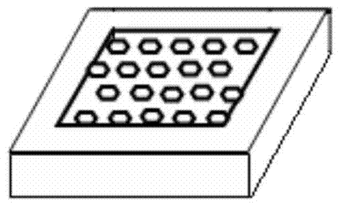
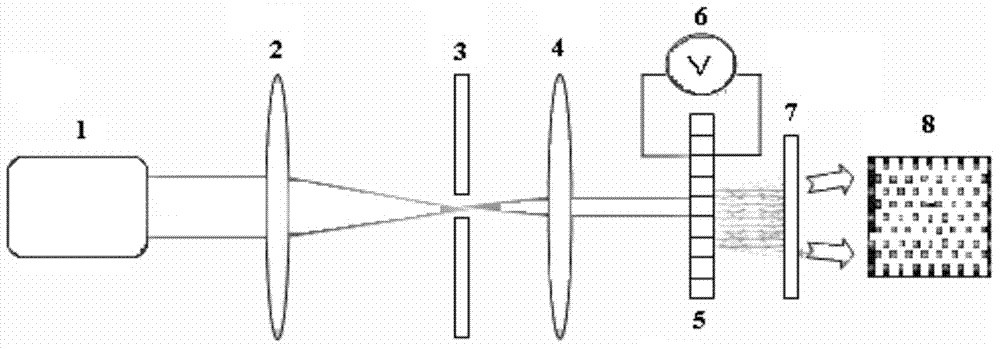
[0022] The two-dimensional submicron photonic crystal phase array optical beam splitter proposed by the present invention mainly utilizes the electro-optical effect and piezoelectric effect of photonic microstructure crystals, and applies an external electric field to modulate the change of crystal refractive index and piezoelectric thickness. , realize the phase change to form a phase array grating, and uniform diffraction beam splitting occurs when the plane light wave passes through the phase grating.

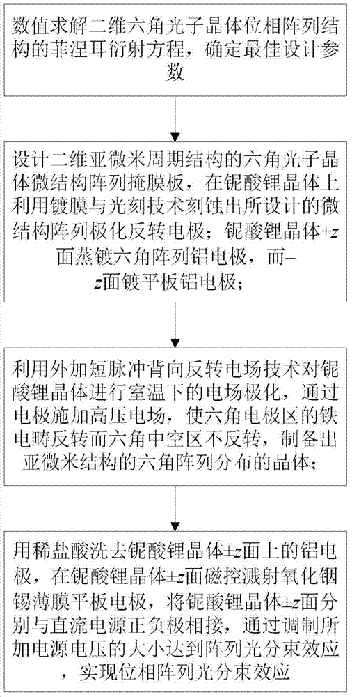
[0023] The manufacture method flow process of the optical beam splitter designed by the present invention is as follows figure 1 As shown, specifically:

[0024] 1) The present invention utilizes the Fresnel diffraction theory and the Fourier transform theory of the secondary phase factor to analyze the Tablot effect diffraction of the two-dimensional photonic micro...


PUM


Abstract

The invention belongs to the technical field of novel electronic devices and light information and relates to a manufacturing method of a submicron photonic crystal phase array light beam splitter. The method comprises the steps that (1) a Fresnel diffraction equation of a two-dimension hexagonal photonic crystal phase array structure is solved, and the optimum designing parameters are determined; (2) a hexagonal photonic crystal microstructural array mask plate of a two-dimension submicron periodic structure is designed, and a microstructural array polarization inversion electrode is etched on a lithium niobate crystal; (3) the lithium niobate crystal is subjected to electric field polarization, and a hexagonal array distribution crystal of a submicron structure is prepared; and (4) aluminum electrodes on the +/-z faces of the lithium niobate crystal are washed off, indium tin oxid thin film flat plate electrodes are subjected to magnetron sputtering on the +/-z faces, the +/-z faces of the lithium niobate crystal are connected to a positive electrode and a negative electrode of a direct-current power supply, the magnitude of voltages is adjusted, and the phase array light beam splitting effect is achieved. The designed light beam splitter has the advantages of being good in beam splitting evenness, large in light spot dot matrix number, high in diffraction efficiency and the like, and information parallel transmission and processing can be achieved.

Description

technical field [0001] The invention belongs to the field of novel optoelectronic devices and the field of optical information, and in particular relates to a manufacturing method of a submicron photonic crystal phase array optical beam splitter. Background technique [0002] In many fields of modern technology such as optical interconnection, optical computing, optical disk storage, optoelectronic technology, image processing and precision measurement, there are more and more requirements to convert the input of information (image or data) into the output of multiple information Realize the parallel transmission and processing of information, thereby increasing the speed. Beam splitters are components that split a beam of light into two or more beams. Traditional planar beam splitters are usually made of metal or dielectric films to distribute optical power in multiple directions. When used, lenses are needed to converge the beams into an array of points, which is difficul...

Claims


Application Information

Patent Timeline
IPC IPC(8): G02B27/10G02F1/03
Inventor 陈云琳张进宏范天伟
Owner BEIJING JIAOTONG UNIV
Why Eureka
Try Eureka