Deep silicon etching method

A technology of deep silicon etching and etching, which is applied in the direction of electrical components, semiconductor/solid-state device manufacturing, circuits, etc., can solve the problem of poor roughness of the etching bottom, reduce the quality of deep silicon etching, and reduce the selection ratio of etching To achieve the effect of inhibiting the formation of micro-mask and even silicon grass, improving the unevenness of the bottom and improving the roughness

Active Publication Date: 2014-06-25
BEIJING NAURA MICROELECTRONICS EQUIP CO LTD
View PDF8 Cites 8 Cited by
  • Summary
  • Abstract
  • Description
  • Claims
  • Application Information

AI Technical Summary

Problems solved by technology

Micromask or silicon grass generation can lead to poor roughness of the bottom of the etch and reduce the quality of deep silicon etching
[0007] In order to avoid the production of micromasks or silicon grass, in the prior art, the etching step is usually carried out at a lower process pressure, but due to the use of a lower process pressure, the silicon etching rate will be reduced, thereby reducing Etching selectivity ratio

Method used


Image

  • Deep silicon etching method
  • Deep silicon etching method
  • Deep silicon etching method

Examples


Embodiment Construction

[0032] In order to enable those skilled in the art to better understand the technical solution of the present invention, the deep silicon etching method provided by the embodiment of the present invention will be described in detail below with reference to the accompanying drawings.

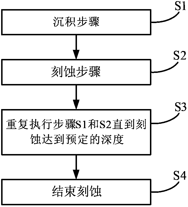
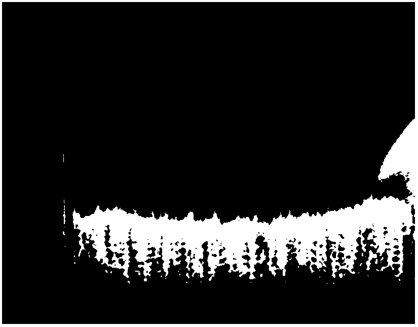
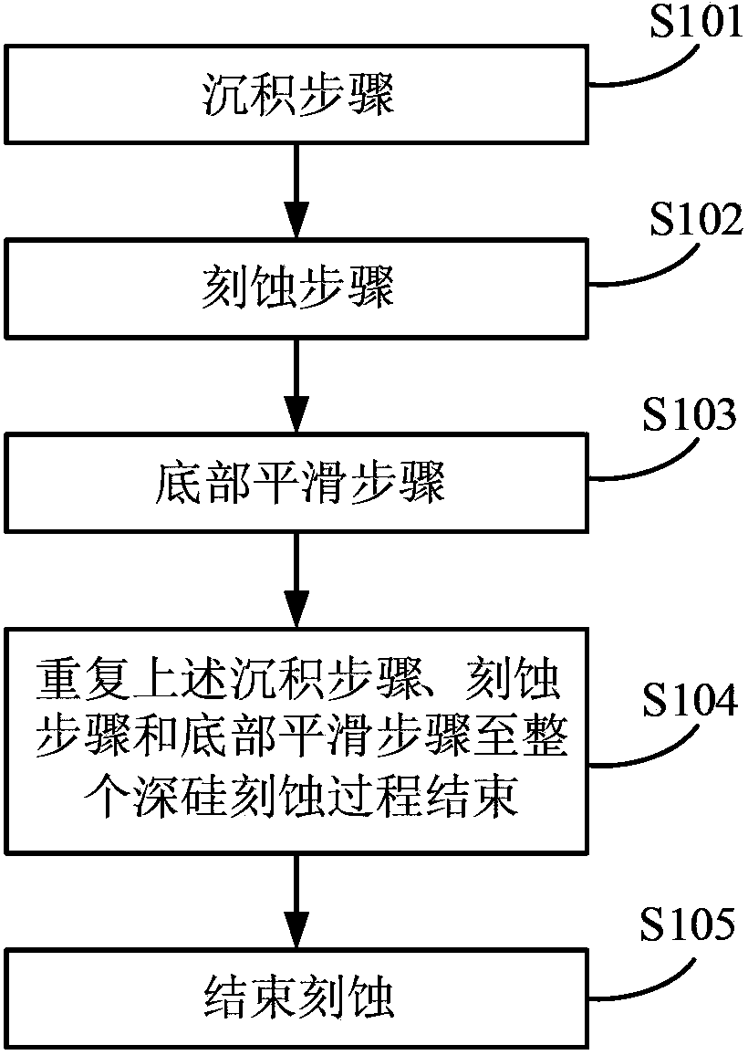
[0033] An embodiment of the present invention provides a deep silicon etching method, the method comprising: a deposition step, forming a protective layer to protect the etched sidewall; an etching step, etching the etched bottom and the etched sidewall; The deposition step and the etching step are repeated until the entire deep silicon etching process ends. In the deep silicon etching method, a bottom smoothing step is also included, the bottom smoothing step is: using a fluorine-containing gas to perform plasma treatment to remove the polymer produced at the bottom of the etching due to deposition; and, the bottom smoothing step adopts The process pressure is less than the process pressure used...


PUM


Abstract

The invention discloses a deep silicon etching method. The deep silicon etching method comprises steps that: a deposition step, a protection layer is generated to protect an etching side wall; an etching step, an etching bottom portion and the etching side wall are etched; the deposition step and the etching step are repeated till the whole deep silicon etching process is over; a bottom portion smoothing step is further included, wherein the bottom portion smoothing step comprises that a fluorine-containing gas is utilized to carry out plasma processing to remove polymers generated because of deposition at the etching bottom portion, the technology pressure employed in the bottom portion smoothing step is smaller than the technology pressure employed in the etching step, at least one bottom portion smoothing step is carried out in the whole deep silicon etching process. Through the deep silicon etching method, gradual increase of the etching bottom polymer is inhibited in the deep silicon etching process, generation of a micro mask layer or silicon grasses is inhibited, and thereby the etching rate of deep silicon etching and the selectivity ratio are improved, and roughness of the etching bottom is ameliorated.

Description

technical field [0001] The invention relates to the field of semiconductor manufacturing, in particular to a deep silicon etching method. Background technique [0002] With MEMS (Micro-Electro-Mechanical Systems, Micro-Electro-Mechanical Systems) devices and MEMS systems being more and more widely used in the automotive and consumer electronics fields, and TSV through hole etching (Through Silicon Etch) technology in the future packaging field With broad prospects, the dry plasma deep silicon etching process has gradually become one of the mainstream processes in the field of MEMS processing and TSV technology. [0003] The main difference between the deep silicon etching process and the general silicon etching process is that the etching depth of the deep silicon etching process is much larger than that of the general silicon etching process, and the etching depth of the deep silicon etching process is generally tens of microns Even hundreds of microns, while the etching d...

Claims


Application Information

Patent Timeline
Patent Type & Authority Applications(China)
IPC IPC(8): H01L21/3065
CPCH01L21/30655H01L21/3065
Inventor 蒋中伟
Owner BEIJING NAURA MICROELECTRONICS EQUIP CO LTD
Why Eureka
Try Eureka