Preparation method for semiconductor device with improved surge current resistance

A semiconductor, anti-surge technology, applied in semiconductor/solid-state device manufacturing, semiconductor devices, circuits, etc., can solve problems such as increased conduction voltage drop, increased device conduction loss, and device damage

Inactive Publication Date: 2014-06-25
HANGZHOU ENNENG TECH
View PDF5 Cites 4 Cited by
  • Summary
  • Abstract
  • Description
  • Claims
  • Application Information

AI Technical Summary

Problems solved by technology

Since there is basically no minority carrier injection phenomenon in the Schottky junction, under harsh working conditions such as surge current conditions, the conduction voltage drop of the traditional TMBS diode increases sharply, and the conduction loss of the device increases rapidly, resulting in device damage.

Method used


Image

  • Preparation method for semiconductor device with improved surge current resistance
  • Preparation method for semiconductor device with improved surge current resistance
  • Preparation method for semiconductor device with improved surge current resistance

Examples


Embodiment Construction

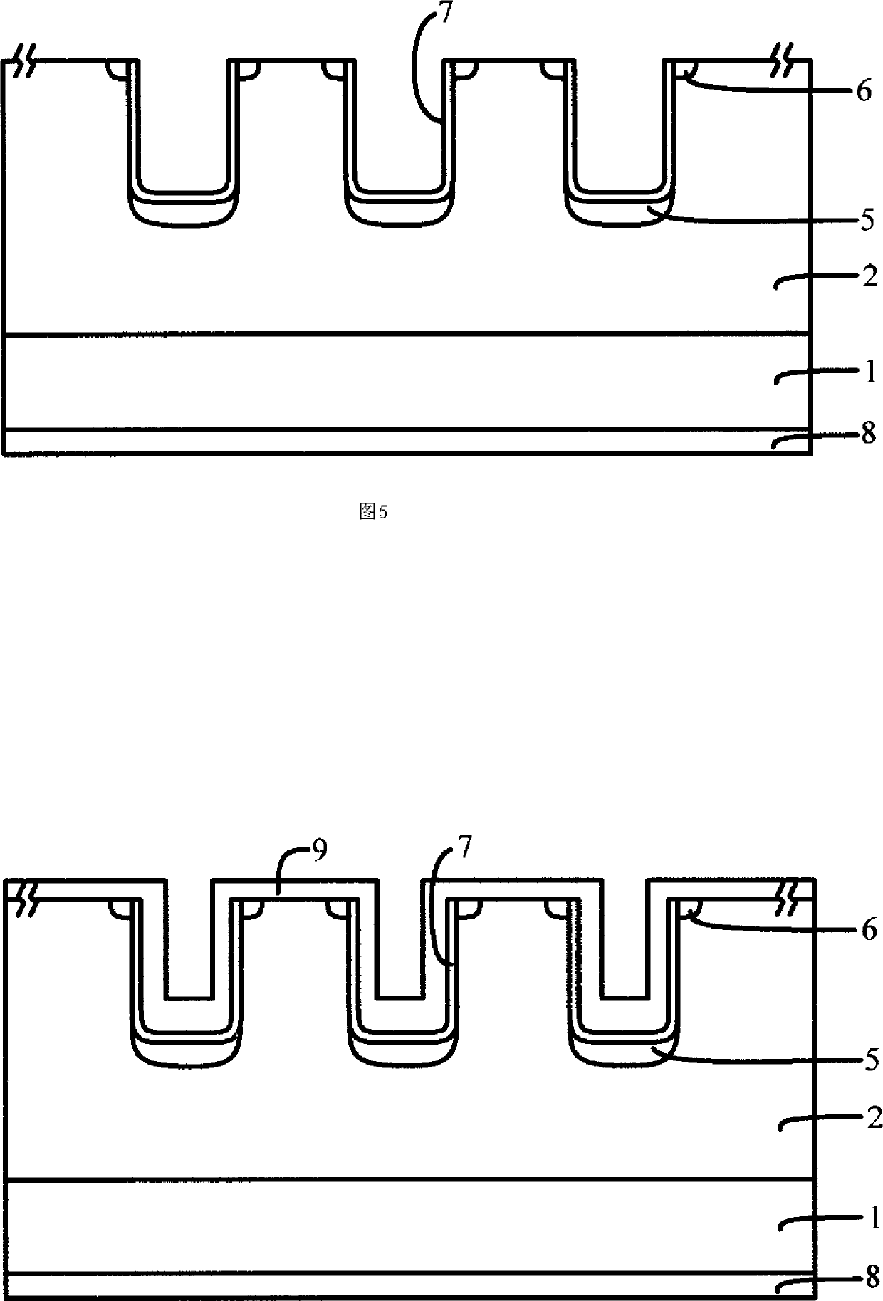
[0023] Image 6 In order to be a cross-sectional view of a semiconductor device with improved anti-surge current capability of the present invention, the following is combined Image 6 The semiconductor device of the present invention will be described in detail.

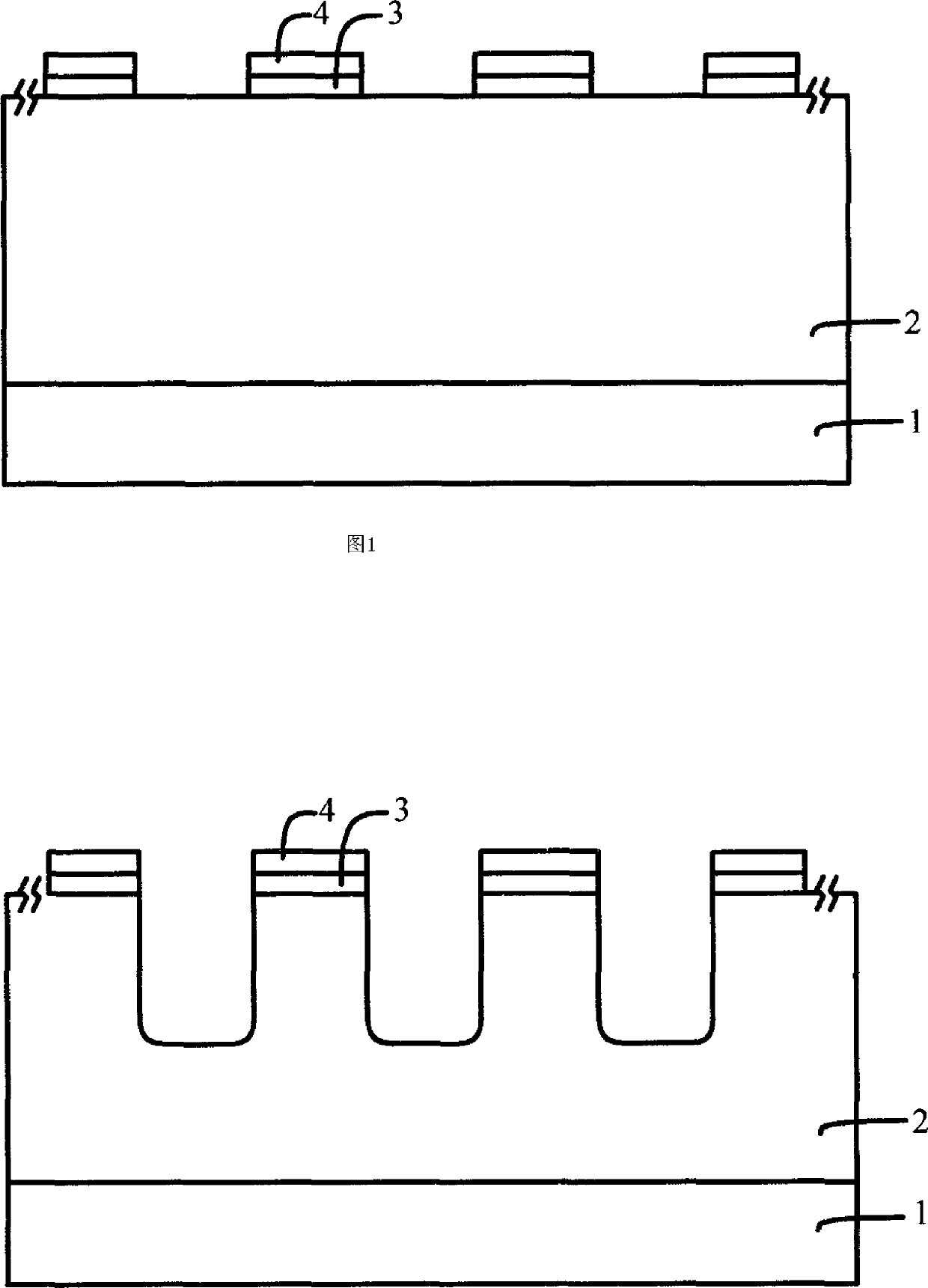
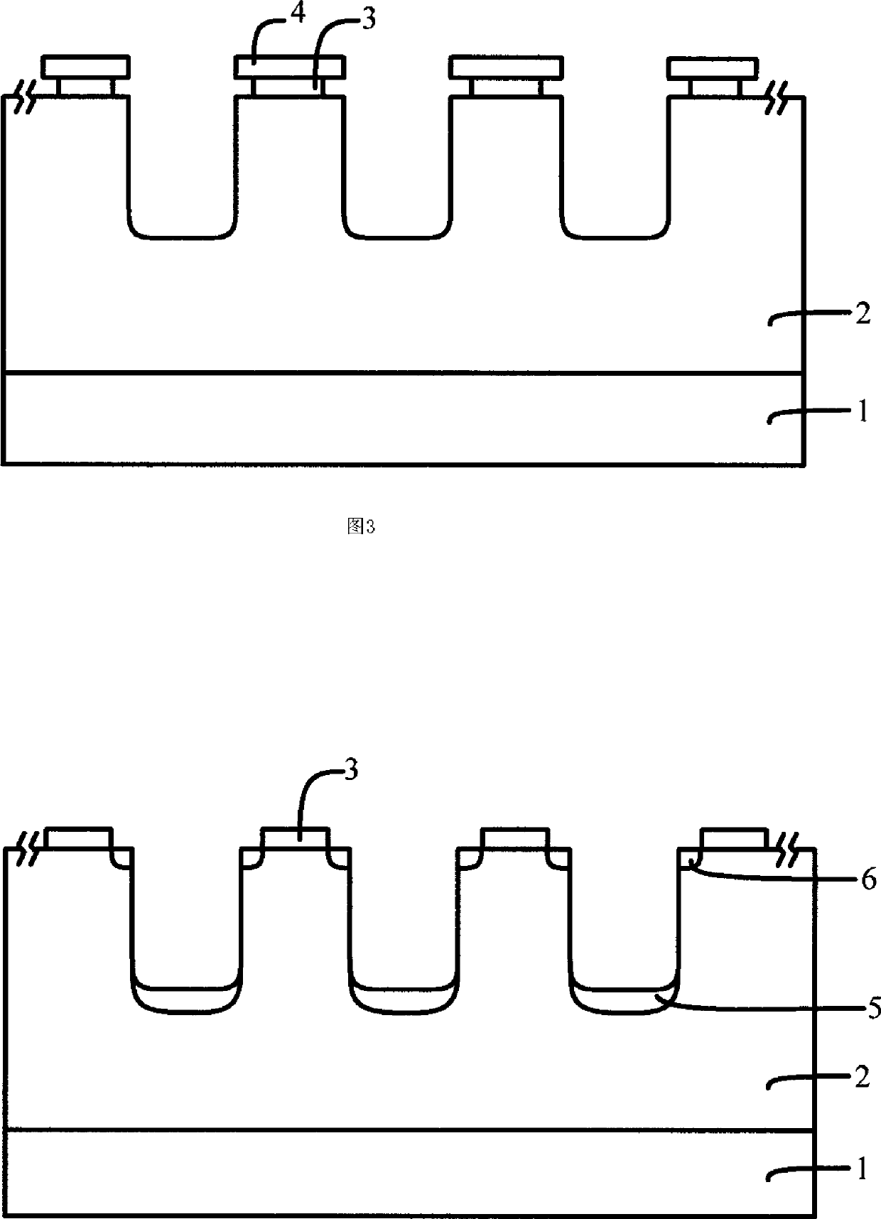
[0024] A semiconductor device with anti-surge current capability, comprising: a substrate layer 1, which is an N conductivity type silicon carbide semiconductor material, and the doping concentration range of the N type material is [1e15 / cm 3 , 1e20 / cm 3 ]; on the upper surface of the substrate layer 1 is the drift layer 2, which is an N conductivity type silicon carbide semiconductor material, its doping concentration is lower than that of the substrate layer 1, and the doping concentration range of the N-type material is [1e13 / cm 3 , 1e19 / cm 3 ], etched by RIE method on the surface of the layer to form a deep groove; ion implantation at the bottom of the trench and on both sides of the mesa forms P-type implant...


PUM


Abstract

The invention discloses a preparation method for a semiconductor device with improved surge current resistance. The semiconductor device is an improved TMBS diode. According to the semiconductor device, metal Cr is utilized to act as an etching mask film to form a deep groove structure on the surface of a SiC drift layer. Wet etching is performed so that line width of the Cr mask film is narrowed, two sides of a mesa which is not etched are exposed to act as an injection mask film to perform Al-ion injection on the surface of the SiC drift layer, and P-type injection regions are formed on the two sides of the mesa. A PN-junction is formed by the injection regions and an N-type drift region. The PN-junction participates in conduction under the condition of high current. The conductance modulation effect is formed by utilizing minority-carrier injection so that the semiconductor device is enabled to have surge current resistance. Besides, a P-injection region can be formed on the bottom part of a groove simultaneously. The bottom part of the groove can be protected by the P-region under the reverse blocking state of the device, the situation that electric field concentration is formed on a non-ideal etching surface can be avoided, early breakdown can be prevented and thus reliability of the device can be enhanced.

Description

technical field [0001] The invention relates to a preparation method of a semiconductor device with improved anti-surge current capability. The semiconductor device of the invention is mainly used in power circuits. Background technique [0002] Silicon carbide semiconductor devices are excellent representatives of next-generation power semiconductor devices. Silicon carbide semiconductor materials have better current conduction and voltage blocking capabilities than first-generation silicon power semiconductor materials, and can achieve very low on-resistance and fast switching time. Therefore, it is suitable for application in the direction of semiconductor power devices. [0003] The anode of the traditional silicon carbide semiconductor device TMBS diode (Trench Metal-Oxide-Semiconductor Barrier Schottky Diode) is a pure Schottky junction, and there is no PN junction. Since there is basically no minority carrier injection phenomenon in the Schottky junction, under hars...

Claims


Application Information

Patent Timeline
Patent Type & Authority Applications(China)
IPC IPC(8): H01L21/329
CPCH01L29/66143H01L29/0623
Inventor 何敏任娜王珏
Owner HANGZHOU ENNENG TECH
Why Eureka
Try Eureka