NP-type CMOS avalanche photodiode with deep N-trap

An avalanche photoelectric, NP-type technology, applied in the field of photoelectric detection, can solve the problems of NP-type APD device speed, response frequency, low bandwidth, slow diffusion speed, etc., and achieve fast diffusion speed, increased diffusion speed, and improved response speed Effect

Active Publication Date: 2014-06-25
CHONGQING UNIV OF POSTS & TELECOMM
View PDF5 Cites 16 Cited by
  • Summary
  • Abstract
  • Description
  • Claims
  • Application Information

AI Technical Summary

Problems solved by technology

However, due to the slow diffusion motion, the rate, response

Method used


Image

  • NP-type CMOS avalanche photodiode with deep N-trap
  • NP-type CMOS avalanche photodiode with deep N-trap
  • NP-type CMOS avalanche photodiode with deep N-trap

Examples


Embodiment Construction

[0019] A non-limiting embodiment is given below in conjunction with the accompanying drawings to further illustrate the present invention.

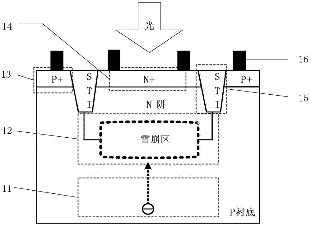
[0020] have to be aware of is, Figure 1 and Figure three Represents only a schematic simplified view of a CMOS APD, therefore the two figures are not drawn to scale.

[0021] Such as Figure 1 Shown is the structural diagram of a conventional NP-type CMOS APD optoelectronic device. A conventional NP-type CMOS APD includes a substrate 11 (typically made of Si material), an avalanche region 12 (typically made of PN structure, the P-type semiconductor is made of boron-doped Si material, and the N-type semiconductor is made of phosphorus Doped Si material), P-type contact 13 (typically, composed of heavily P-doped Si material), N-type contact 14 (typically, composed of heavily N-doped Si material), STI15 (also known as Shallow trench isolation, typically made of SIO2 material), electrode 16 (typically made of Al material). It should be...


PUM


Abstract

The invention discloses an NP-type CMOS avalanche photodiode with a deep N-trap. The NP-type CMOS avalanche photodiode comprises a P-type substrate, an N-trap layer and an avalanche area. The N-trap layer and the avalanche area are arranged on the P-type substrate, the avalanche area is arranged between the P-type substrate and the N-trap layer to form a PN junction, a light absorbing layer is further arranged between the P-type substrate and the avalanche area, the light absorbing layer is the deep N-trap arranged on the P-type substrate, and the dosage concentration of the deep N-trap is larger than that of the P-type substrate. By means of the NP-type CMOS avalanche photodiode, the rate, the frequency response and bandwidth of avalanche photodiode devices are improved.

Description

technical field [0001] The invention relates to the technical field of photoelectric detection, to the structure of a photoelectric device, in particular to a deep N-well NP-type CMOS avalanche photodiode. Background technique [0002] Avalanche photodiode, also known as APD (avalanche photodiode), works on the principle that the photogenerated carriers (hole-electron pairs) generated by the photoelectric effect are rapidly accelerated when moving in the high electric field region (reverse voltage on the PN junction) , One or more collisions may occur during the movement, and secondary and tertiary new hole-electron pairs are generated through the impact ionization effect, resulting in an avalanche multiplication effect, which rapidly increases the number of carriers, thereby forming a relatively large optical signal current. In terms of low light intensity, high sensitivity and high speed applications, APD devices are very attractive. For example, long-distance optical comm...

Claims


Application Information

Patent Timeline
IPC IPC(8): H01L31/107H01L31/0352
CPCH01L31/035272H01L31/107
Inventor 王巍王川颜琳淑胡洁王婷杜超雨王振袁军
Owner CHONGQING UNIV OF POSTS & TELECOMM
Why Eureka
Try Eureka