Method for depositing high k gate medium on graphene material and application

A technology of graphene and gate dielectric, which is applied in the direction of metal material coating process, coating, gaseous chemical plating, etc., can solve the problems of increasing the overall thickness of the gate dielectric, the influence of the process, and the reduction of carrier mobility. Increase the scope of application and solve the effect of selectivity

Inactive Publication Date: 2014-07-02
PEKING UNIV
View PDF5 Cites 6 Cited by
  • Summary
  • Abstract
  • Description
  • Claims
  • Application Information

AI Technical Summary

Problems solved by technology

[0008] (1) None of them can accurately control the specific position of graphene surface pretreatment, and can only perform overall treatment on the entire silicon wafer or the entire graphene film, which will inevitably have a certain impact on the subsequent process
[0009] (2)O 3 or NO 2 The treatment method also causes new and additional defects in graphene, so that the performance (such as: carrier mobility) is significantly reduced
[0010] (3) The buffer layer or Al seed layer will increase the overall thickness of the gate dielectric, making it difficult to meet the requirements of high-quality ultra-thin gate dielectric

Method used


Image

  • Method for depositing high k gate medium on graphene material and application
  • Method for depositing high k gate medium on graphene material and application
  • Method for depositing high k gate medium on graphene material and application

Examples


Embodiment 1

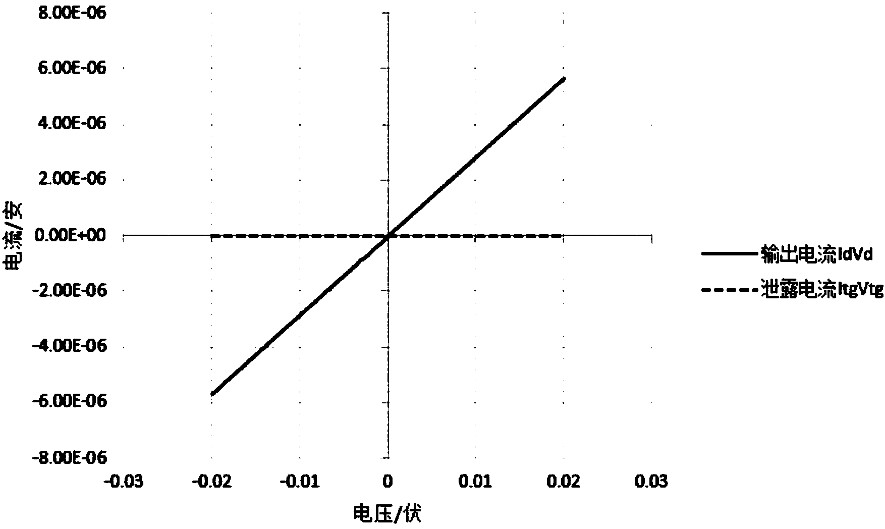
[0031] Example 1: ALD deposition of high-k dielectric on the surface of single-layer graphene

[0032] Preparation of graphene materials

[0033] Using transparent tape and highly oriented graphite flakes, graphene was prepared by mechanical exfoliation, and the substrate was 300nm thermally grown SiO on low-resistance silicon 2 .

[0034] Characterization of graphene materials.

[0035] Observe the shape and color of the prepared graphene under an optical microscope, and preliminarily determine its surface flatness and the number of graphite layers. Raman scattering spectrum was used for further characterization, the number of layers of graphene was determined according to the height ratio of G peak and 2D peak, and the surface defects of graphene were judged according to the height of D peak. Single-layer and defect-free graphene is selected as the sample, that is, the ratio of the G peak to the 2D peak of the Raman spectrum is about 0.5, and there is no obvious D peak. ...

Embodiment 2

[0042] Example 2: ALD deposition of high-k dielectric on the surface of exfoliated multilayer graphene

[0043] Preparation of graphene materials.

[0044] Using transparent tape and highly oriented graphite flakes, graphene was prepared by mechanical exfoliation, and the substrate was 300nm thermally grown SiO on low-resistance silicon 2 .

[0045] Characterization of graphene materials.

[0046] Observe the shape and color of the prepared graphene under an optical microscope, and preliminarily determine its surface flatness and the number of graphite layers. Raman scattering spectrum was used for further characterization, the number of layers of graphene was determined according to the height ratio of G peak and 2D peak, and the surface defects of graphene were judged according to the height of D peak. The graphene with multiple layers and no defects is selected as the sample, that is, the ratio of the G peak to the 2D peak of the Raman spectrum is greater than 0.5, and t...

Embodiment 3

[0053] Example 3: ALD deposition of high-k dielectric on CVD graphene

[0054] Preparation of graphene materials.

[0055] Under the catalysis of copper foil, graphene is grown by CVD, and the process of PMMA wet transfer is used to obtain uniform single-layer graphene.

[0056] Characterization of graphene materials.

[0057] Observe the shape and color of the prepared graphene under an optical microscope to preliminarily determine the uniformity of the graphene surface. Raman scattering spectrum was used for further characterization, the number of layers of graphene was determined according to the height ratio of G peak and 2D peak, and the surface defects of graphene were judged according to the height of D peak. Single-layer and defect-free graphene is selected as the sample, that is, the ratio of the G peak to the 2D peak of the Raman spectrum is about 0.5, and there is no obvious D peak.

[0058] The samples were pretreated by electron beam scanning.

[0059] Put the...


PUM

PropertyMeasurementUnit
thicknessaaaaaaaaaa
thicknessaaaaaaaaaa
relative permittivityaaaaaaaaaa

Abstract

The invention discloses a method for depositing a high k gate medium on a graphene material and application, and belongs to the technical field of integrated circuits. The method includes the steps of firstly selecting the graphene material which is smooth in surface and free of defects or less in defects to serve as a substrate sample used for depositing the high k medium; placing the substrate sample in a vacuum cavity of a scanning electron microscope, conducting vacuumizing to the range from 5E-4 to 1E-7, and scanning the surface of the substrate sample through a low-energy focusing electron beam for 30 s to 5 min, wherein the acceleration voltage of the low-energy electron beam ranges from 1 kV to 15 kV; depositing a thin amorphous carbon film on the surface of the substrate sample in the scanning process, wherein the thickness of the thin amorphous carbon film ranges from 0.3 nm to 3 nm; placing the substrate sample processed through the electron beam into an ALD device, and conducting high k medium material deposition. According to the method and the application, medium deposition can still be conducted on the surface of the material without hanging keys through the ALD device, a continuous, uniform and compact high-quality material is obtained, and the application range of the ALD device is widened.

Description

technical field [0001] The invention belongs to the technical field of integrated circuits, and in particular relates to a method for depositing a high-k gate dielectric on the surface of a graphene material or a device structure based on the graphene material. Background technique [0002] In the preparation process of field effect transistor (FET) and radio frequency field effect transistor (RF-FET) based on carbon nanotubes, graphene and graphene-like materials, the preparation of gate dielectric is a key process, high performance FET and RF -FET requires a high-quality, ultra-thin gate dielectric as a prerequisite. Atomic layer deposition (ALD) is the most commonly used method for depositing high-k gate dielectrics. It has the advantages of high deposition quality and precise controllable deposition thickness. ALD uses self-limiting surface chemical reactions to deposit insulating dielectric materials layer by layer on the surface of the target substrate with an atomic-...

Claims


Application Information

Patent Timeline
Patent Type & Authority Applications(China)
IPC IPC(8): H01L21/02H01L21/285C23C16/455C23C16/04
CPCC23C16/455H01L21/02H01L21/285H01L21/0228C23C16/40C23C16/45525H01L29/66477
Inventor 叶青傅云义郭剑贾越辉魏子钧张亮任黎明黄如张兴
Owner PEKING UNIV
Why Eureka
Try Eureka