
A method for forming a gate dielectric layer on the surface of graphene and preparing a transistor

A graphene surface, gate dielectric layer technology, applied in coating, metal material coating process, semiconductor/solid state device manufacturing, etc. problem, to achieve the effect of excellent performance and excellent performance

Active Publication Date: 2020-06-16
HUAWEI TECH CO LTD
View PDF5 Cites 0 Cited by
  • Summary
  • Abstract
  • Description
  • Claims
  • Application Information

AI Technical Summary

Problems solved by technology

[0006] However, the use of common water-based ALD methods to grow top-gate dielectric layers on the surface of graphene has the following problems: due to the hydrophobic surface of graphene, it is difficult for water molecules to adsorb on the surface of graphene, which makes it difficult to form a film or film of the grown gate dielectric Poor compactness leads to inability to insulate
However, the introduction of the seed layer in this method will, on the one hand, increase the overall thickness of the top gate dielectric layer, making it difficult to meet the requirements of an ultra-thin gate dielectric layer; on the other hand, the existence of the seed layer reduces the purity of the gate dielectric layer and increases the interface effect. The performance of graphene FETs is affected

Method used


Image

  • A method for forming a gate dielectric layer on the surface of graphene and preparing a transistor
  • A method for forming a gate dielectric layer on the surface of graphene and preparing a transistor
  • A method for forming a gate dielectric layer on the surface of graphene and preparing a transistor

Examples


Embodiment 1

[0074] Embodiment 1: A gate dielectric layer 60 of aluminum oxide is formed on the surface of graphene 20, such as Figure 4 As shown, it specifically includes the following steps:

[0075] S201. Using a micromechanical exfoliation method to peel off the graphene 20 from the graphite, and form the graphene on a 300 nm silicon oxide substrate.

[0076] S202 , placing the substrate 10 formed with the graphene 20 in step S201 in an 85% ammonia atmosphere to adsorb ammonia molecules.

[0077] S203, placing the graphene 20 adsorbed ammonia in S202 in the ALD reaction chamber, and passing water vapor 40 under room temperature conditions, so that the surface of the graphene 20 adsorbs water molecules.

[0078]S204. Raise the temperature of the ALD reaction chamber to 300° C., and introduce trimethylaluminum vapor, and the trimethylaluminum vapor reacts with the water molecules adsorbed on the surface of the graphene 20 to form a single layer 50 of the gate dielectric layer 60 of alu...

Embodiment 2

[0081] Embodiment 2: Form a gate dielectric layer 60 of hafnium dioxide on the surface of graphene 20, such as Figure 5 As shown, it specifically includes the following steps:

[0082] S301. Form graphene 20 by chemical vapor deposition, and transfer graphene 20 to a quartz surface by using PMMA (Polymethylmethacrylate).

[0083] S302, placing the substrate 10 formed with the graphene 20 in step S301 in a 90% hydrogen chloride environment to absorb hydrogen chloride molecules.

[0084] S303, placing the graphene 20 adsorbed with hydrogen chloride in step 302 in the ALD reaction chamber, and passing water vapor 40 at room temperature, and the surface of the graphene 20 adsorbs water molecules.

[0085] S304. Raise the temperature of the ALD reaction chamber to 300° C., and introduce hafnium tetrachloride vapor, and the hafnium tetrachloride vapor reacts with the water molecules adsorbed on the surface of graphene 20 to form a monolayer of hafnium dioxide gate dielectric layer...


PUM


Abstract

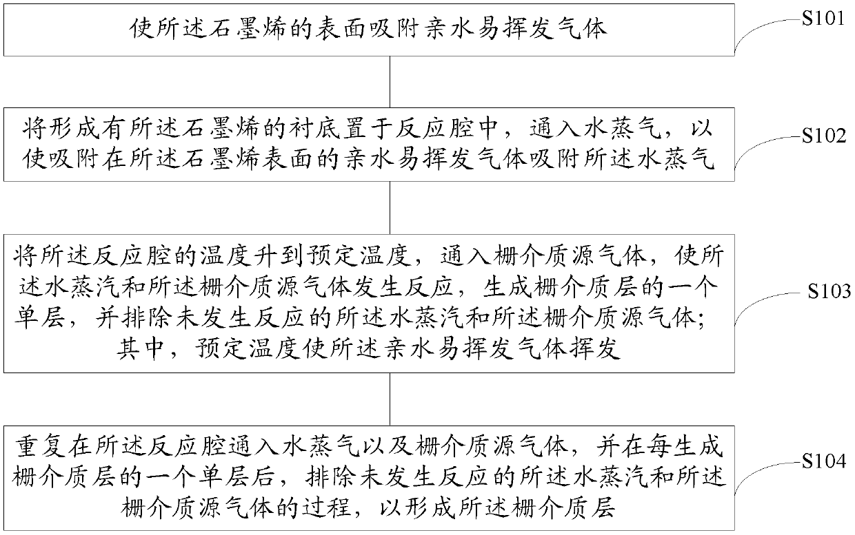
This invention discloses a method for forming a gate dielectric on the surface of graphene and producing a field effect transistor and relates to the field of electronic device technology, wherein a large area of high quality, uniform gate dielectric layer is formed. The method comprises the following: allowing the graphene surface to absorb a hydrophilic volatile gase; placing the substrate on which graphene is formed in an ALD reaction chamber and injecting water vapor to be absorbed by the hydrophilic volatile gas on the surface of the graphene surface; raising the temperature of the ALD reaction chamber to a predetermined temperature then injecting the gate dielectric source gas to allow said vapor and gate dielectric source gas to react, producing a monolayer of a gate dielectric layer and allowing the hydrophilic volatile gas to evaporate; and repeating the process of injecting water vapor and the gate dielectric source gas into the ALD reaction chamber to form multiple monolayers of a gate dielectric layer, thereby forming a gate dielectric layer. The method is used in fabricating FETs.

Description

technical field [0001] The invention relates to the technical field of electronic components, in particular to a method for forming a gate dielectric layer on the surface of graphene and preparing field effect transistors (Field Effect Transistors, FET for short). Background technique [0002] Graphene is a two-dimensional film material formed by carbon atoms arranged in a regular hexagonal honeycomb lattice. Its unique electronic structure endows graphene with many superior and peculiar electrical properties. When the sheet-like graphene carrier concentration is n=10 12 cm -3 , the mobility can theoretically reach 200,000cm 2 V -1 the s -1 , is 140 times that of silicon materials, and the conductivity can reach 10 6 S / m is known as the next-generation electronic material that can replace silicon. [0003] Due to its excellent electrical properties, graphene is widely used in many electronic devices. Among them, the most representative electronic device is the field ...

Claims


Application Information

Patent Timeline
IPC IPC(8): H01L21/31C23C16/40
CPCC23C16/40H01L21/31
Inventor 梁晨张臣雄
Owner HUAWEI TECH CO LTD
Learn More