Substrate integrated waveguide filter

A substrate-integrated waveguide and filter technology, which is applied to waveguide-type devices, electrical components, circuits, etc., can solve the problems of increased loss, large area occupied by substrate-integrated waveguide resonators, and increased filter volume, and achieve loss Low, small size, effect of improving selectivity

Inactive Publication Date: 2014-07-02
UNIV OF ELECTRONICS SCI & TECH OF CHINA
View PDF5 Cites 12 Cited by
  • Summary
  • Abstract
  • Description
  • Claims
  • Application Information

AI Technical Summary

Problems solved by technology

[0003] In order to meet the higher requirements of the modern communication system on the size and selectivity of the filter, the design of the traditional substrate integrated waveguide filter structure generally obtains more transmission zero points by increasing the number of resonator stages to improve the out-of-band Selectivity, but limited by the large footprint of the substrate integrated waveguide resonator, as the number of resonators increases, not only the size of the filter will increase, but also its loss will increase accordingly, so the selection of the communication system direct impact on performance, noise figure, gain, and sensitivity

Method used


Image

  • Substrate integrated waveguide filter
  • Substrate integrated waveguide filter
  • Substrate integrated waveguide filter

Examples


Embodiment Construction

[0014] The specific embodiments of the present invention will be further described below in conjunction with the accompanying drawings.

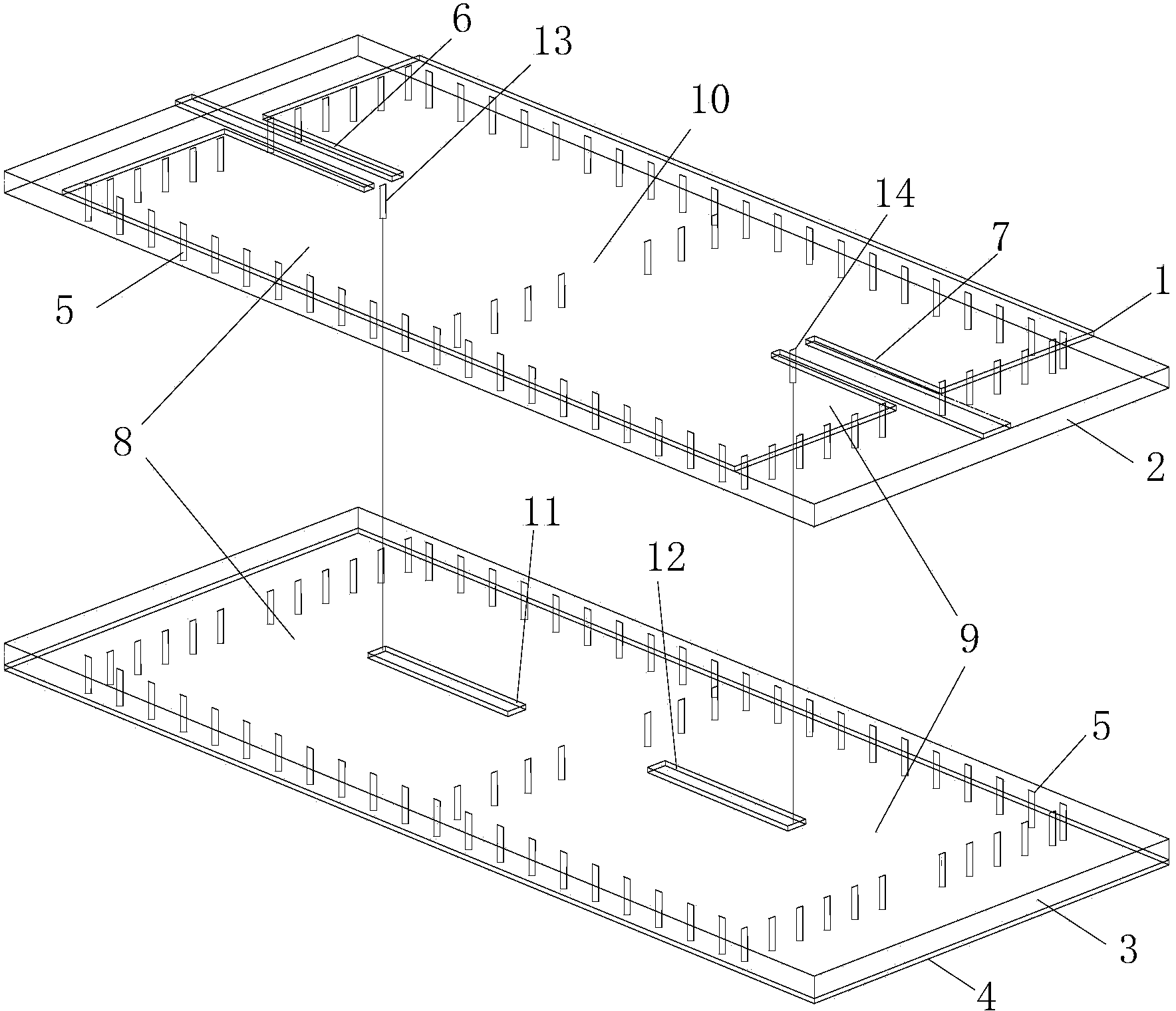
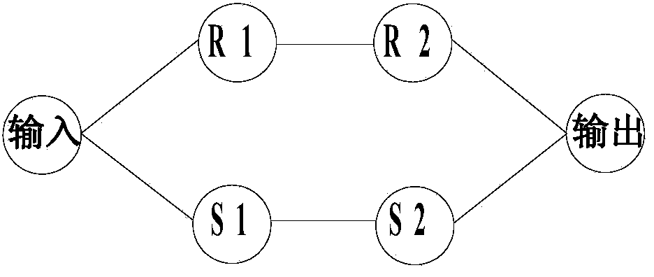
[0015] Such as figure 1 As shown, the substrate-integrated waveguide filter includes a first metal layer 1, a first dielectric substrate 2, a second dielectric substrate 3, a second metal layer 4, and a metallized through-hole array 5 stacked sequentially from top to bottom. , the first metal layer 1 is provided with a coplanar waveguide input end 6 and a coplanar waveguide output end 7, the metallized via hole array 5 runs through the first dielectric substrate 2, the second dielectric substrate 3 and is connected with the first metal layer 1. The second metal layer 4 together forms a first resonant cavity 8 and a second resonant cavity 9, the first resonant cavity 8 and the second resonant cavity 9 are coupled to each other through an inductive coupling window 10, and the first dielectric substrate 2 A first ribbon-shaped coupling unit 11...


PUM


Abstract

The invention discloses a substrate integrated waveguide filter which is high in selectivity, small in size and low in loss. The substrate integrated waveguide filter comprises a first metal layer, a first dielectric substrate, a second dielectric substrate, a second metal layer and a metallization through hole array, the first metal layer, the first dielectric substrate, the second dielectric substrate, the second metal layer and the metallization through hole array are sequentially stacked from top to bottom, and a first band-shaped coupling unit and a second band-shaped coupling unit are arranged between the first dielectric substrate and the second dielectric substrate. By means of the substrate integrated waveguide filter, the LTCC technology is adopted for integrating the band-shaped coupling units into resonant cavities of the substrate integrated waveguide filter, a signal transmission channel can be added without increasing the number of the resonant cavities, a transmission null point can be accordingly obtained in an attenuation band, and the selectivity of the filter is improved; meanwhile, the position of the transmission null point can be flexibly controlled by adjusting the resonant frequencies of the band-shaped coupling units, more stages of the resonant cavities are not needed, and the substrate integrated waveguide filter has the advantages of being small in size, light in weight and low in loss. The substrate integrated waveguide filter is suitable for popularization and application in the microwave millimeter wave technical field.

Description

technical field [0001] The invention relates to the field of microwave and millimeter wave technology, in particular to a substrate integrated waveguide filter. Background technique [0002] The filter is one of the most basic basic circuits in the communication system, and its performance is directly related to the performance of the entire system. Traditional filters are generally divided into planar microstrip or stripline structure filters and metal waveguide structure filters. Although planar microstrip or stripline structure filters are easy to integrate, they have large radiation loss and low Q value. Although metal waveguide structure filters have the characteristics of low loss, high Q value, and good selectivity, they are large in size and complex in processing and debugging, which is not conducive to integration with active circuit substrates. The filter based on the substrate integrated waveguide technology not only retains the advantages of easy integration an...

Claims


Application Information

Patent Timeline
Patent Type & Authority Applications(China)
IPC IPC(8): H01P1/208H01P1/203
Inventor 徐自强张根郭俊宇夏红程革胜杨邦朝
Owner UNIV OF ELECTRONICS SCI & TECH OF CHINA
Why Eureka
Try Eureka