Method for transferring graphene on hard substrate with PDMS transition layer

A technology of hard substrate and transition layer, applied in chemical instruments and methods, inorganic chemistry, non-metallic elements, etc., can solve the problems of graphene damage and low transfer efficiency, and achieve the effect of stable process and low cost

Active Publication Date: 2014-07-16
SHANGHAI INST OF MICROSYSTEM & INFORMATION TECH CHINESE ACAD OF SCI
View PDF4 Cites 9 Cited by
  • Summary
  • Abstract
  • Description
  • Claims
  • Application Information

AI Technical Summary

Problems solved by technology

[0006] In view of the above-mentioned shortcoming of prior art, the object of the present invention is to provide a kind of method that graphene is transferred to the hard substrate with PDMS transition layer, has solved the transfer efficiency low in the past graphene transfer process, graphene vulnerable to damage

Method used


Image

  • Method for transferring graphene on hard substrate with PDMS transition layer
  • Method for transferring graphene on hard substrate with PDMS transition layer
  • Method for transferring graphene on hard substrate with PDMS transition layer

Examples


Embodiment 1

[0037] Transfer of graphene on copper foil to glass substrate with PDMS transition layer

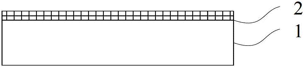
[0038] First, a high-quality graphene continuous film was grown on a 2 cm × 2 cm copper foil by the CVD method. Generally, after the CVD method, there are graphene 2 on the upper and lower sides of the copper foil 1, the lower side is particularly scattered, and the upper side is fine. The graphene film under the copper foil can be polished off or etched away by some means, such as oxygen plasma. In this embodiment, the graphene on the lower layer of the copper foil is removed. formed as Figure 1a structure shown.

[0039] Then use the following steps to transfer:

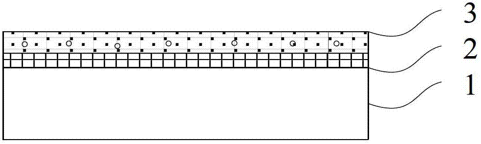
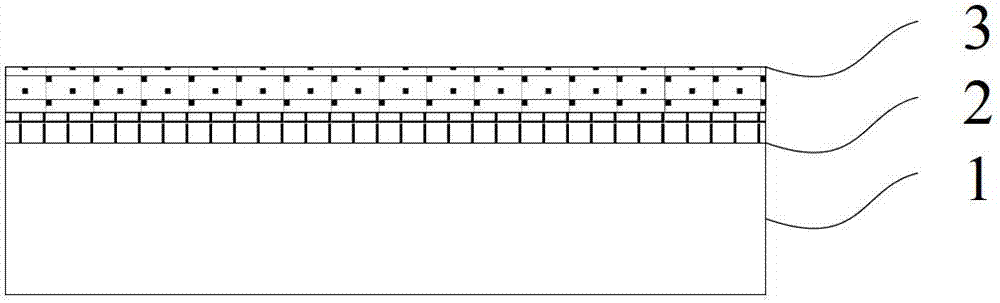
[0040] a) Spin-coat PDMS glue 3 with a thickness of 20 μm on the copper foil 1 after growing graphene 2; spin-coating is to disperse the PDMS glue evenly on the surface of the copper foil with a glue spreader, and the glue spreader can set the speed, generally About 4000 rpm;

[0041] PDMS (polydimethylsiloxane polydim...

Embodiment 2

[0048] Transfer of graphene grown on electroplated copper to Si / SiO with PDMS transition layer 2 Substrate

[0049] First, a copper film with a thickness of about 10 μm is electroplated on a silicon wafer with an oxide layer of about 300 nm; continuous graphene is grown on the copper film formed by the electroplating above by using a CVD process.

[0050] The graphene grown on electroplated copper was then transferred to Si / SiO with PDMS transition layer 2 The substrate process is as follows:

[0051] a) Manually apply a layer of PDMS glue on the above-mentioned electroplated copper, and do not exceed the edge of the above-mentioned copper film when applying PDMS glue;

[0052] b) Put the above-mentioned copper film coated with PDMS glue into a vacuum drying oven to evacuate and suck out the air bubbles in the PDMS glue;

[0053] c) Put the above copper film on a hot plate at 100°C and bake it for 50 minutes to cure the PDMS glue to form a PDMS transition layer on the copper ...


PUM


Abstract

The invention discloses a method for transferring graphene on a hard substrate with a PDMS transition layer. The method comprises the following steps that PDMS glue coats an original substrate coated with graphene; the PDMS glue is solidified to form the PDMS transition layer; plasma treatment is carried out on the PDMS transition layer and the hard substrate, and then the PDMS transition layer and the hard substrate are pressed lightly and bonded; the bonded hard substrate is put into corrosive liquid to etch off the original substrate; a graphene/PDMS transition layer/hard substrate combined body is rinsed repeatedly by using deionized water and is blown dried, and the graphene transferred on the hard substrate with the PDMS layer is obtained. The method is simple in operation, low in cost and wide in application range, the graphene material is not prone to damage in the transferring process, the graphene can be efficiently and stably transferred on the hard substrate with the PDMS transition layer, and the method and a semiconductor technology can be combined to be used for preparing graphene electronic devices.

Description

technical field [0001] The invention belongs to the technical field of semiconductor materials. In particular it relates to a method for transferring graphene onto a rigid substrate with a PDMS transition layer. Background technique [0002] Graphene is a planar monoatomic layer film material formed by carbon atoms arranged in a two-dimensional regular hexagonal honeycomb lattice. Since graphene has a series of properties such as outstanding thermal conductivity and mechanical properties, high electron mobility, and half-integer quantum Hall effect, since it was first discovered in 2004, graphene has attracted widespread attention from the scientific community and set off a wave. boom in research. [0003] At present, graphene has been proved to be applicable to the preparation of various electronic devices, such as molecular sensors, field effect transistors, flexible electronic devices and so on. The fabrication of graphene-based electronic devices usually requires the ...

Claims


Application Information

Patent Timeline
Patent Type & Authority Applications(China)
IPC IPC(8): H01L21/02C01B31/04C01B32/194
CPCH01L21/02422H01L21/02439H01L21/02527
Inventor 李铁梁晨王文荣王跃林
Owner SHANGHAI INST OF MICROSYSTEM & INFORMATION TECH CHINESE ACAD OF SCI
Why Eureka
Try Eureka