Preparation method of ultraviolet light emitting diode device

A technology of light-emitting diodes and devices, which is applied in semiconductor devices, electrical components, circuits, etc., can solve problems such as uneven etching depth, poor uniformity of light output efficiency of on-chip devices, and influence on device reliability, so as to eliminate the risk of damage and improve The effect of luminous efficiency

Active Publication Date: 2016-09-28
INST OF SEMICONDUCTORS - CHINESE ACAD OF SCI
View PDF3 Cites 3 Cited by
  • Summary
  • Abstract
  • Description
  • Claims
  • Application Information

AI Technical Summary

Problems solved by technology

[0004] However, if the pits are prepared using the dry etching process reported in Reference 1, there will be great challenges
First of all, in order to enhance the plasmon coupling effect, it is hoped that the bottom of the pit is close to the active area. On the other hand, if the bottom of the pit is closer to the active area, it is easier to etch the active area during dry etching. Causes damage to the active area, thereby reducing the internal quantum efficiency of the UV light-emitting diode device, and at the same time affecting the reliability of the device and shortening the service life
Since plasma dry etching has a certain damage depth, it is difficult to avoid damage to the active region by this process
Secondly, the etching speed of dry etching is not easy to control, resulting in uneven etching depth on the chip and uneven coupling effect of plasmons, and poor uniformity of light extraction efficiency of on-chip devices.

Method used


Image

  • Preparation method of ultraviolet light emitting diode device
  • Preparation method of ultraviolet light emitting diode device
  • Preparation method of ultraviolet light emitting diode device

Examples


Embodiment Construction

[0031] In order to make the object, technical solution and advantages of the present invention clearer, the present invention will be further described in detail below in conjunction with specific embodiments and with reference to the accompanying drawings.

[0032] The invention proposes a preparation method of an ultraviolet light-emitting diode device, which can effectively and accurately control the distance from the active region to the metal plasmon, and eliminates the risk of damage to the active region during the process, thereby enhancing The effect of plasmonic technology on improving the luminous efficiency of ultraviolet light-emitting diode devices was demonstrated.

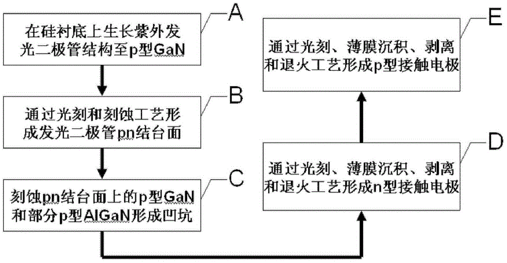
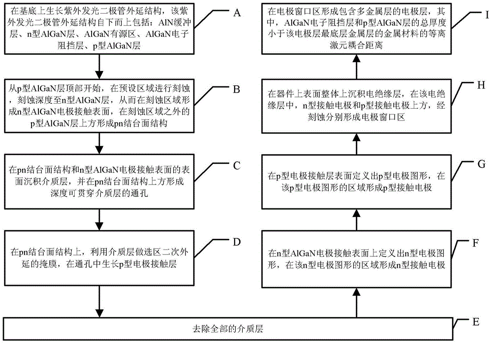
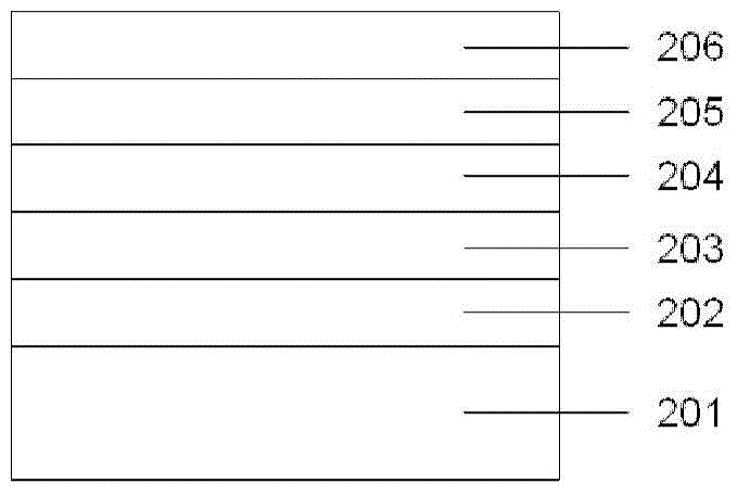
[0033] In an exemplary embodiment of the present invention, a method for manufacturing an ultraviolet light emitting diode device is provided. figure 2 It is a flowchart of a method for manufacturing an ultraviolet light emitting diode device according to an embodiment of the present invention. Ple...


PUM

PropertyMeasurementUnit
thicknessaaaaaaaaaa
thicknessaaaaaaaaaa
emission peakaaaaaaaaaa

Abstract

The invention provides a preparation method of an ultraviolet light-emitting diode device. The preparation method of the ultraviolet light-emitting diode device is characterized in that a distance between an active region and a metal plasmon is effectively and accurately controlled as the total thickness of an AlGaN electron barrier layer 205 and a p-type AlGaN layer 206 is smaller than the plasmon coupling distance of metal materials of a metal layer of the bottommost layer of an electrode layer, the risk that the active region is damaged in process engineering is eliminated and the luminous efficiency of the ultraviolet light-emitting diode device is improved.

Description

technical field [0001] The invention relates to the technical field of optoelectronic devices, in particular to a method for preparing an ultraviolet light-emitting diode device. Background technique [0002] Ultraviolet light-emitting diode devices have attracted much attention because of their huge potential application value in many fields such as excitation of white light, biochemical detection, sterilization, environmental purification, polymer curing, and short-distance safe communication. Compared with the traditional ultraviolet light source mercury lamp, AlGaN-based ultraviolet light-emitting diode devices have the advantages of long life, low working voltage, adjustable wavelength, environmental protection, good directionality, rapid switching, shock resistance and moisture resistance, light and flexible, etc. With the deepening of research work , will become the mainstream light source for new UV applications in the future. However, due to the difficulty in epita...

Claims


Application Information

Patent Timeline
Patent Type & Authority Patents(China)
IPC IPC(8): H01L33/00
CPCH01L33/0066H01L33/007H01L33/0075H01L33/145H01L33/20
Inventor 张韵孙莉莉闫建昌王军喜李晋闽
Owner INST OF SEMICONDUCTORS - CHINESE ACAD OF SCI
Why Eureka
Try Eureka