High-power LED lamp with heat radiated through ceramics

一种LED灯具、高功率的技术,应用在照明和加热设备、发光元件的半导体器件、照明装置等方向,能够解决影响LED芯片发光效率、芯片发光区发光不均匀、N级焊锡层38过长等问题,达到提高LED发光效率、增加光穿透层面积、最佳发光效率的效果

Active Publication Date: 2014-07-23
JIANGSU HOWELL TRANSPORTATION GRP CO LTD
View PDF5 Cites 2 Cited by
  • Summary
  • Abstract
  • Description
  • Claims
  • Application Information

AI Technical Summary

Problems solved by technology

[0008] 1. The N-type electrode 37 is located far away from the P-type electrode 34 in the horizontal direction. The N-type electrode 37 has strict requirements on the position design of the PCB board 39 below it, which affects the packaging quality rate
[0009] 2. The position of the N-type electrode 37 is much higher than that of the P-type electrode 34, resulting in a large gap between it and the PCB board 39 below, and it is easy to make the N-level solder layer 38 too long during soldering, resulting in false soldering or detachment Occurrence of welding
[0010] 3. In order to allow welding of the N-type electrode 37 and the PCB board 39 below it, a large part of the light-emitting area needs to be removed, which affects the luminous efficiency of the LED chip
[0011] 4. The electrode area is not large enough, which affects the injection current efficiency and then affects the luminous efficiency of the LED chip
[0012] 5. P-type electrodes and N-type electrodes are located on both sides of the chip, resulting in different electron flow paths, such as Figure 36 , resulting in uneven resistance and uneven light emission in the light-emitting area of ​​the chip, which affects the luminous efficiency of the LED chip

Method used


Image

  • High-power LED lamp with heat radiated through ceramics
  • High-power LED lamp with heat radiated through ceramics
  • High-power LED lamp with heat radiated through ceramics

Examples


Embodiment Construction

[0079] Combine below Figure 1 to Figure 34 , the present invention is further described:

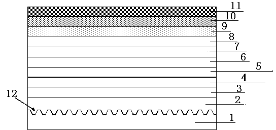
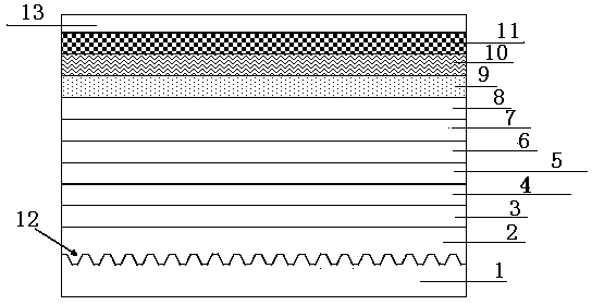
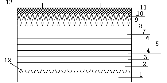
[0080] like figure 1 As shown, the substrate 1 is a carrier, generally made of materials such as sapphire, silicon carbide, silicon, GaAs, AlN, ZnO or GaN.

[0081] On the substrate 1, a layer of concave-convex surface 12 is firstly formed by etching. The concave-convex surface 12 can reduce the total reflection of light in the chip and increase the light extraction rate.

[0082] The buffer layer 2 is a transition layer on which high-quality N, P, quantum wells and other materials are grown.

[0083] LED is composed of pn structure, buffer layer 2, N-type layer 3, N-type confinement layer 4, P-type confinement layer 6 and P-type layer 7 are to form P and N-type materials required for making LED. The light-emitting area layer 5 is the light-emitting area of ​​the LED, and the color of the light is determined by the material of the active area.

[0084] P-type ohmic contact layer 8 ...


PUM


Abstract

The invention relates to a high-power LED lamp with heat radiated through ceramics. The high-power LED lamp comprises a ceramic radiating base (6), a circuit board is fixed to one face of the ceramic radiating base (6), a white light LED flip chip (5) is connected to the circuit board, a nontransparent lampshade is fixed to the position above the white light LED flip chip (5), outward-protruding radiating fins (61) are arranged on the other face of the ceramic radiating base (6), and the radiating fins (61) are made of ceramic materials. Due to the fact that the radiating fins and the ceramic radiating base are made of ceramic materials, heat produced by the white light LED flip chip can be rapidly absorbed and radiated through high conductivity and high radiation physical properties of the ceramic materials, it is ensured that the white light LED flip chip is in the constant low temperature state and can work stably and continuously, and therefore the service life of the LED lamp can be prolonged.

Description

technical field [0001] The application date of the present invention is February 27, 2012, the application number is: 201210044889.4, and the divisional application of the invention patent application named "a high-power LED lamp using ceramic heat dissipation". The invention relates to an LED lamp, in particular to a high-power LED lamp using ceramics for heat dissipation. Background technique [0002] Due to the large heat dissipation of LED lamps, if the heat dissipation cannot be carried out in time, especially high-power LEDs will burn out electronic components after a long time, affecting the normal use and life of LED lamps. The heat dissipation devices on the market now usually use metal heat dissipation, but metal heat dissipation is not as effective as ceramic materials. [0003] In addition, the advantages of using a sapphire substrate are good chemical stability, no absorption of visible light, moderate price, and relatively mature manufacturing technology, so i...

Claims


Application Information

Patent Timeline
Patent Type & Authority Applications(China)
IPC IPC(8): H01L33/64H01L33/38H01L33/50F21Y115/10
CPCF21Y2101/00H01L33/38H01L33/40H01L33/505H01L33/641H01L33/642H01L2933/0016H01L2933/0041H01L2933/0075
Inventor 俞国宏
Owner JIANGSU HOWELL TRANSPORTATION GRP CO LTD
Why Eureka
Try Eureka