High-thermal-conductivity ceramic substrate containing filling copper columns and manufacturing process thereof
A technology of high thermal conductivity ceramics and ceramic substrates, applied in the direction of multilayer circuit manufacturing, electrical connection formation of printed components, electrical connection of printed components, etc., can solve problems such as poor thermal conductivity, achieve the effect of improving controllability and simplifying the process
- Summary
- Abstract
- Description
- Claims
- Application Information
AI Technical Summary
Problems solved by technology
Method used
Image

Examples
preparation example Construction
[0045] A preparation process for a high thermal conductivity ceramic substrate containing filled copper pillars, comprising the following steps:
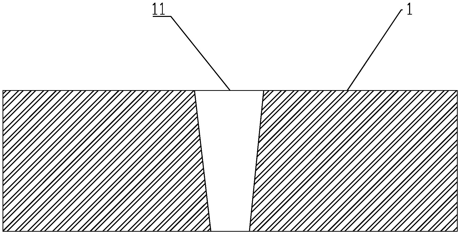
[0046] 1) By adjusting the diameter and energy of the laser spot, drill holes along the thickness direction of the ceramic sheet. The diameter of the upper opening of the hole is 100-200 μm, and the diameter of the lower opening is 30-80 μm;
[0047] After this step processing, it is formed as figure 1 In the shown structure, a hole 11 is formed on the ceramic sheet 1, the hole is a tapered hole, the diameter of the upper opening is 100-200 μm, and the diameter of the lower opening is 30-80 μm;
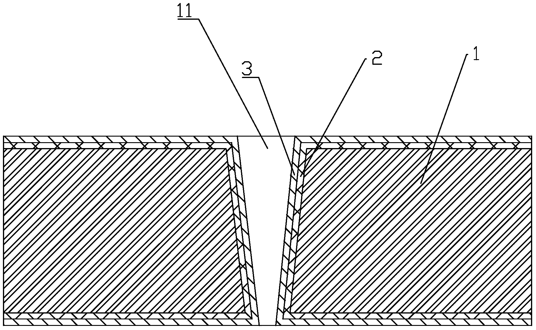
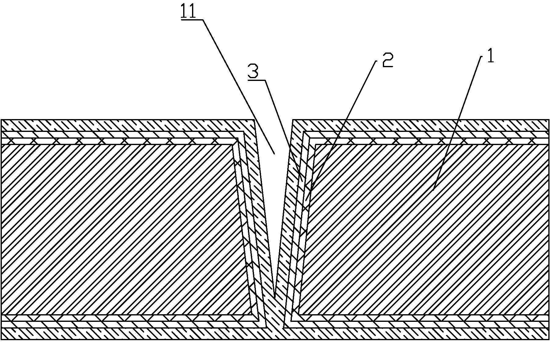
[0048] 2) Sputter the buffer layer and the conductive layer sequentially on the perforated ceramic sheet;
[0049] After this step processing, it is formed as figure 2 In the shown structure, after the ceramic sheet 1 containing the hole 11 is sputtered, a structure comprising a buffer layer 2 and a conductive layer 3 is formed, the cond...
Embodiment 1
[0063] A preparation process for a high thermal conductivity ceramic substrate containing filled copper pillars, comprising the following steps:
[0064] 1) By adjusting the laser spot diameter and energy, drill 12 holes along the thickness direction of the 0.1mm thick aluminum nitride ceramic sheet (the surface size of the ceramic sheet is 7mm×7mm), and the 12 holes are evenly distributed in a matrix of 3×4 On the ceramic sheet, the diameter of the upper opening of a single hole is 180 μm, and the diameter of the lower opening is 80 μm;
[0065] 2) Sputter the Ti / W buffer layer (the thickness of the buffer layer: 400 ?, the mass ratio of Ti and W is 1:1) and the conductive layer Cu of 450 ? sequentially on the perforated ceramic plate;
[0066] 3) DC electroplating copper for 0.5h, so that the lower opening of the hole is closed, and a blind hole is obtained;
[0067] 4) Continue DC electroplating of Cu3h, and the electroplating is single-sided electroplating, so that the bl...
Embodiment 2
[0069] A preparation process for a high thermal conductivity ceramic substrate containing filled copper pillars, comprising the following steps:
[0070] 1) By adjusting the laser spot diameter and energy, drill 12 holes along the thickness direction of the 0.38mm thick aluminum nitride ceramic sheet (the surface size of the ceramic sheet is 7mm×7mm), and the 12 holes are evenly distributed in a matrix of 3×4 On the ceramic sheet, the diameter of the upper opening of the hole is 120 μm, and the diameter of the lower opening is 40 μm;
[0071] 2) Sputter the W / Mo buffer layer (the thickness of the buffer layer: 300 ?, the mass ratio of W and Mo is 1:1) and the conductive layer Cu of 300 ? sequentially on the perforated ceramic plate;
[0072] 3) DC electroplating copper for 0.5h, so that the lower opening of the hole is closed, and a blind hole is obtained;
[0073] 4) Continue DC electroplating for Cu2.5h, and the electroplating is single-sided electroplating, so that the bli...
PUM
| Property | Measurement | Unit |
|---|---|---|
| Upper mouth diameter | aaaaa | aaaaa |
| Lower mouth diameter | aaaaa | aaaaa |
| Thickness | aaaaa | aaaaa |
Abstract
Description
Claims
Application Information
 - R&D
- Intellectual Property
- Life Sciences
- Materials
- Tech Scout
- Unparalleled Data Quality
- Higher Quality Content
- 60% Fewer Hallucinations
Browse by: Latest US Patents, China's latest patents, Technical Efficacy Thesaurus, Application Domain, Technology Topic, Popular Technical Reports.
© 2025 PatSnap. All rights reserved.Legal|Privacy policy|Modern Slavery Act Transparency Statement|Sitemap|About US| Contact US: help@patsnap.com