Preparation method of polycrystalline silicon thin film, polycrystalline silicon thin film transistor and array substrate

A technology of polysilicon thin film and thin film transistor, which is applied in the direction of transistor, semiconductor/solid-state device manufacturing, electric solid-state device, etc. It can solve the problems of low crystal quality, poor stability, and limiting the electrical performance of thin-film transistor devices, etc.

Inactive Publication Date: 2014-08-06
BOE TECH GRP CO LTD
View PDF5 Cites 28 Cited by
  • Summary
  • Abstract
  • Description
  • Claims
  • Application Information

AI Technical Summary

Problems solved by technology

[0005] However, as a gas laser, the excimer laser has relatively poor stability, and the prepared polysilicon grains have relatively poor uniformity, resulting in poor uniformity of electrical characteristics of thin film transistors.
In addition, the usua...

Method used


Image

  • Preparation method of polycrystalline silicon thin film, polycrystalline silicon thin film transistor and array substrate
  • Preparation method of polycrystalline silicon thin film, polycrystalline silicon thin film transistor and array substrate
  • Preparation method of polycrystalline silicon thin film, polycrystalline silicon thin film transistor and array substrate

Examples


Embodiment Construction

[0020] The following will clearly and completely describe the technical solutions in the embodiments of the present invention with reference to the accompanying drawings in the embodiments of the present invention. Obviously, the described embodiments are only some, not all, embodiments of the present invention. Based on the embodiments of the present invention, all other embodiments obtained by persons of ordinary skill in the art without making creative efforts belong to the protection scope of the present invention.

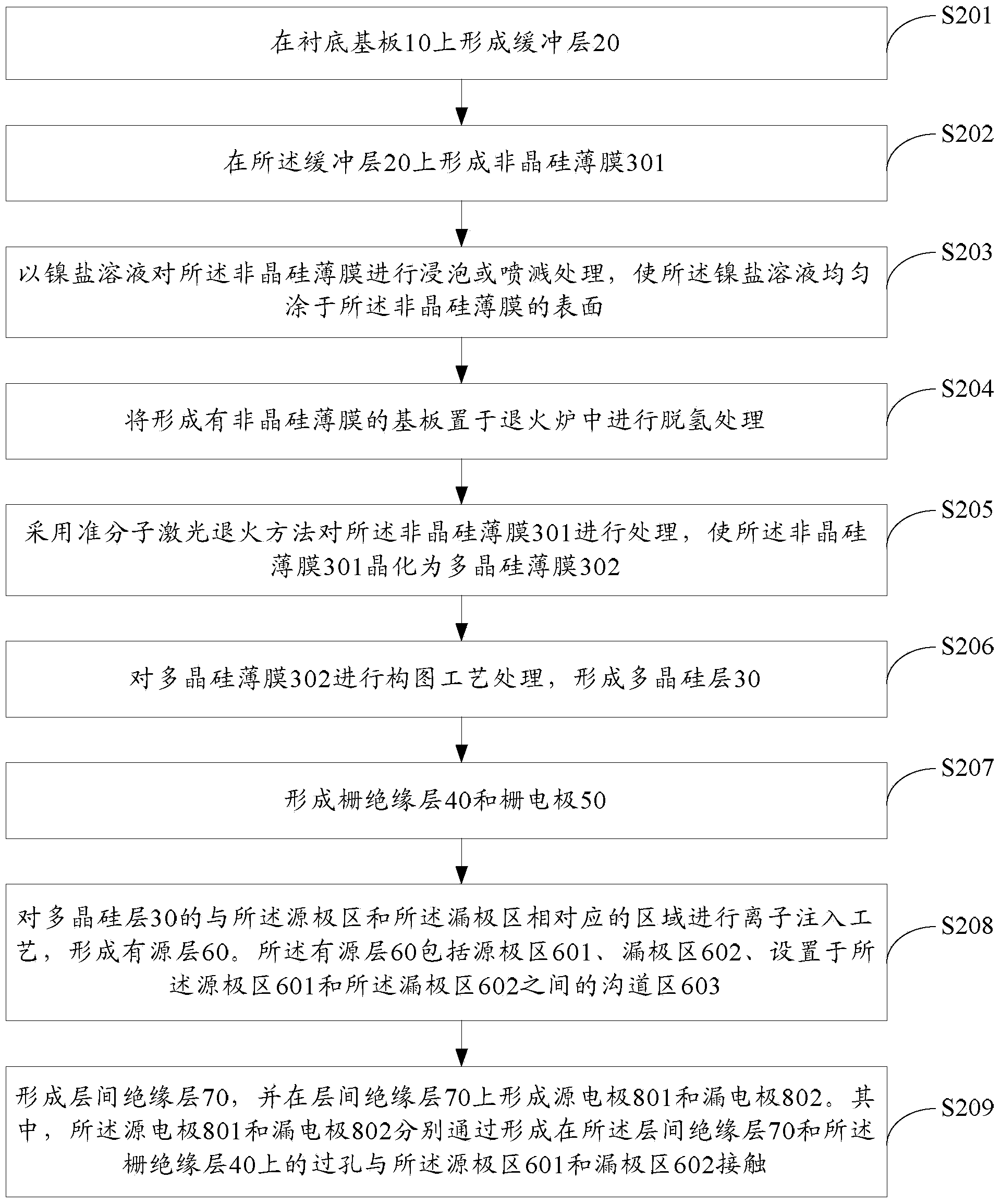
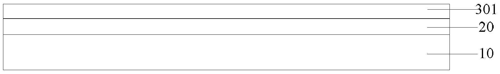
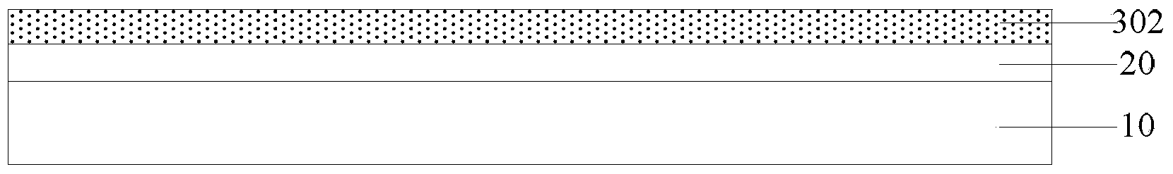
[0021] An embodiment of the present invention provides a method for preparing a polysilicon thin film, comprising: forming an amorphous silicon thin film on a base substrate; using an excimer laser annealing method to treat the amorphous silicon thin film, so that the amorphous silicon thin film crystallized into a polysilicon film; further, after forming the amorphous silicon film, before adopting the excimer laser annealing method to process the amorphous sil...


PUM


Abstract

The embodiment of the invention provides a preparation method of a polycrystalline silicon thin film, a polycrystalline silicon thin film transistor and an array substrate and relates to the technical field of display. By means of the preparation method, polycrystalline silicon crystals are uniform, the grain size is increased, crystal quality is improved, and therefore the electrical properties of the thin film transistor are improved. The preparation method of the polycrystalline silicon thin film comprises the steps that an amorphous silicon thin film is formed on a substrate; the amorphous silicon thin film is treated through an excimer laser annealing method, so that the amorphous silicon thin film is crystallized into the polycrystalline silicon thin film. Furthermore, after the amorphous silicon thin film is formed and before the amorphous silicon thin film is treated though the excimer laser annealing method, the preparation method further comprises the steps that the surface of the amorphous silicon thin film is subjected to nickel salt solution treatment, so that a nickel salt solution is uniformly smeared on the surface of the amorphous silicon thin film. The method is used for preparation of the polycrystalline silicon thin film, the low-temperature polycrystalline silicon thin film transistor and the array substrate requiring that the uniformity of the polycrystalline silicon crystals is improved, the grain size is increased, and crystal quality is improved.

Description

technical field [0001] The invention relates to the field of display technology, in particular to a method for preparing a polysilicon thin film, a method for preparing a low-temperature polysilicon thin film transistor, and a method for preparing an array substrate. Background technique [0002] Low Temperature Poly-Silicon-Thin Film Transistor (LTPS-TFT) display has the advantages of high resolution, fast response, high brightness, high aperture ratio, etc., and because of the characteristics of LTPS, it has high Electron mobility; in addition, the peripheral drive circuit can also be produced on the glass substrate at the same time to achieve the goal of system integration, save space and cost of the drive IC, and reduce product defect rate. [0003] At present, the low-temperature polysilicon thin film transistor includes an active layer, a gate insulating layer, a gate electrode, a source electrode, and a drain electrode arranged on a substrate; the active layer include...

Claims


Application Information

Patent Timeline
IPC IPC(8): H01L21/02H01L21/268H01L29/786H01L21/336
CPCH01L21/02H01L21/268H01L29/786H01L29/6675H01L21/02675H01L27/1214H01L29/78672
Inventor 刘政
Owner BOE TECH GRP CO LTD
Why Eureka
Try Eureka