Preparation method of lubricating film
A technology of lubricating thin film and thin film layer is applied in the field of preparation of lubricating thin film, which can solve the problems of high cost, high production cost, and the resolution cannot be well solved, and achieves the effect of satisfying pattern transfer, high resolution and low cost.
- Summary
- Abstract
- Description
- Claims
- Application Information
AI Technical Summary
Problems solved by technology
Method used
Image

Examples
Embodiment 1
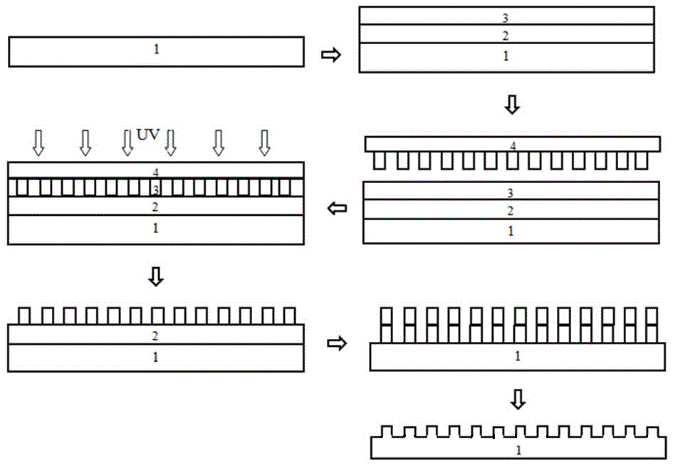
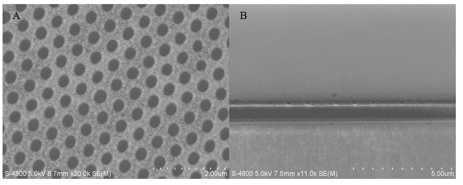
[0044] Embodiment 1: A preparation method of a lubricating film, using ultraviolet hardening imprint lithography (UV-NIL), depositing a silicon-doped diamond-like film on a silicon substrate to prepare a nanometer pattern.
[0045] See attached figure 1 First, the surface of the film layer 1 is treated, and the dust and foreign matter on the surface are blown off with high-purity nitrogen gas for about 1 minute; then the SU-8 photoresist is spin-coated on the surface of the film layer with a thickness of about 500nm, and the spin The sample coated with SU-8 photoresist was exposed under a 1000W ultraviolet lamp for 1 minute, and then the exposed sample was cured by heating at 110°C for 5 minutes to form an intermediate layer 2; then, the cured sample was spin-coated with UV curable adhesive, The thickness is 200nm to form a UV-curable nano-imprint adhesive layer 3; then cover the entire sample with a soft imprint film 4 with a structure, and expose the fully covered sample to ...
Embodiment 2
[0048] Embodiment 2: A method for preparing a lubricating film, using ultraviolet hardening imprint lithography (UV-NIL), depositing a silicon-doped diamond-like film on the surface of a warped sapphire substrate to prepare a nano-pattern.
[0049] First, the surface of the curved substrate is treated, and the dust and foreign matter on the surface are blown off with high-purity nitrogen for about 1 minute; then the SU-8 photoresist is spin-coated on the surface of the film layer with a thickness of about 400nm, and the spin-coating The sample of SU-8 photoresist was exposed under a 1000W ultraviolet lamp for 1 minute, and then the exposed sample was cured by heating at 110°C for 5 minutes to form an intermediate layer; then, the cured sample was spin-coated with UV curable adhesive, with a thickness of 150nm to form a UV-curable nano-imprint adhesive layer; then cover the entire sample with a soft imprint film plate with a structure, and expose the fully covered sample to a 10...
PUM
| Property | Measurement | Unit |
|---|---|---|
| Thickness | aaaaa | aaaaa |
| Thickness | aaaaa | aaaaa |
Abstract
Description
Claims
Application Information