Method for preparing copper cylinder salient points

A technology of bumps and copper pillars, which is applied in the field of preparing copper pillar bumps, can solve the problems of increasing the difficulty of preparation and the complexity of graphics, it is not suitable for the preparation of large-diameter copper pillar bumps, and the electroplating leads cannot be completely removed, etc., so as to improve the quality Efficiency, reduced complexity, and reduced process steps

Active Publication Date: 2014-08-13
NAT CENT FOR ADVANCED PACKAGING
View PDF4 Cites 8 Cited by
  • Summary
  • Abstract
  • Description
  • Claims
  • Application Information

AI Technical Summary

Problems solved by technology

[0003] In the prior art, most of the copper pillar bumps are prepared on the chip, and then the chip with the copper pillar bumps is bonded to the substrate or PCB. In this process, the copper pillar bumps are formed on the chip. However, its diameter and height are greatly limited. At the same time, due to the electroplating of copper pillar bumps on the wafer, its efficiency and cost are relatively high, and it is not suitable for preparing copper pillar bumps with large diameters and high aspect ratios.
[0004] At the same time, the existing substrate bump technology adopts the method of electroplating leads, and each pad under the bump to be electroplated must lead out an electroplating lead to ensure its conductivity, which increases the difficulty of preparation and the complexity of graphics degree
At the same time, after the electroplating is completed, the electroplating lead cannot be completely removed, which further increases the complexity of the process

Method used


Image

  • Method for preparing copper cylinder salient points
  • Method for preparing copper cylinder salient points
  • Method for preparing copper cylinder salient points

Examples


Embodiment Construction

[0029] In order to make the object, technical solution and advantages of the present invention clearer, the present invention will be described in further detail below in conjunction with specific embodiments and with reference to the accompanying drawings.

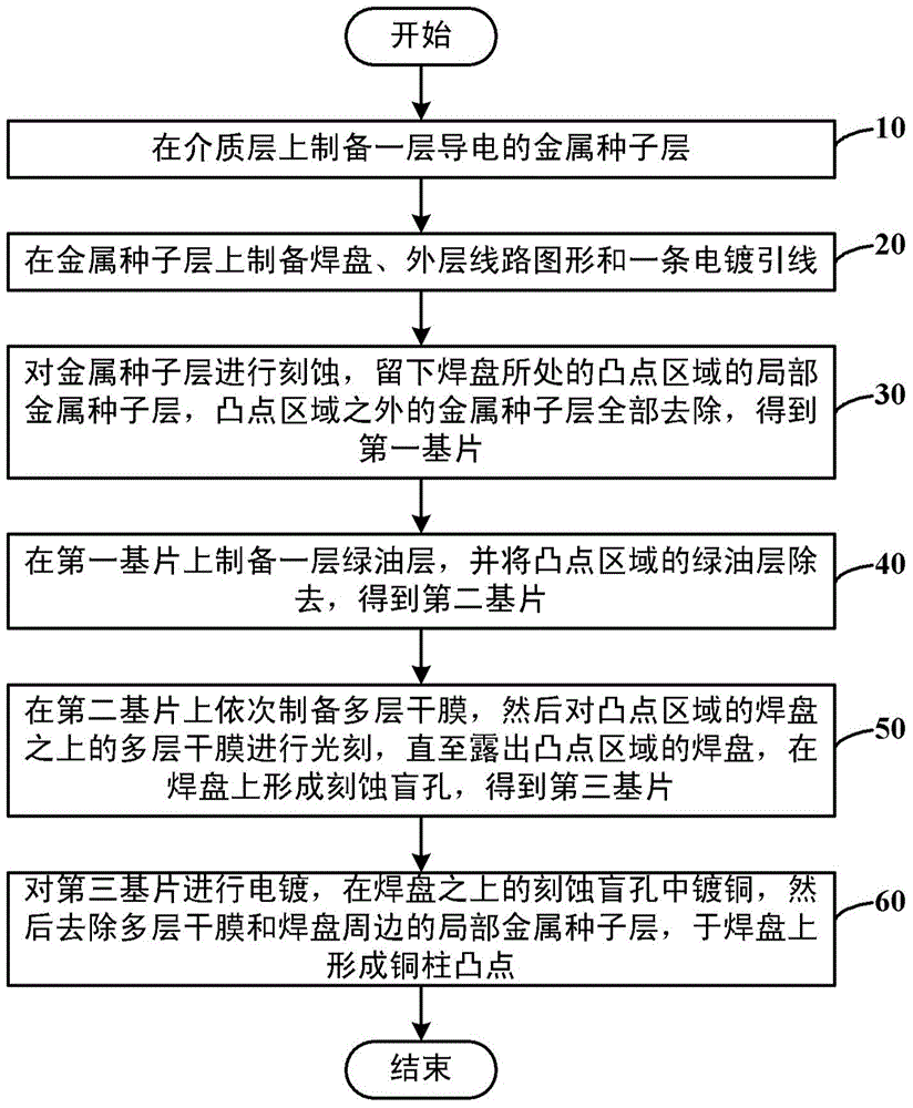
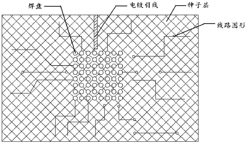
[0030] The method for preparing copper pillar bumps provided by the present invention is to form pillar-shaped copper bumps by electroplating on a substrate or a PCB, and use local metal seed layer technology and multi-layer photosensitive dry film technology to realize the preparation of pillar-shaped bumps without complicated electroplated leads. Such as figure 1 as shown, figure 1 It is a flowchart of a method for preparing copper pillar bumps according to an embodiment of the present invention, and the method includes the following steps:

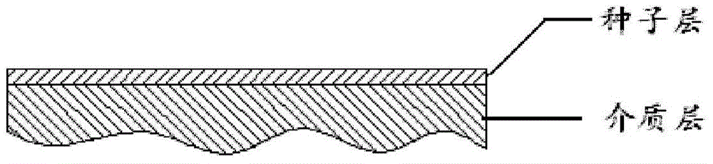
[0031] Step 10: preparing a conductive metal seed layer on the dielectric layer;

[0032] Wherein, preparing a layer of conductive metal seed layer on the dielectric layer is to...


PUM


Abstract

The invention discloses a method for preparing copper cylinder salient points. With the adoption of the local metal seed layer technology and the multilayer sensitive dry film technology, the method includes the steps that a conductive metal seed layer is prepared on a dielectric layer; a bonding pad, an outer-layer circuit pattern and an electroplating lead are prepared on the metal seed layer; the metal seed layer is etched, a local metal seed layer of a salient point region where the bonding pad is located is reserved, the portions, except for the salient point region, of the metal seed layer are all removed, and therefore a first substrate is obtained; a green oil layer is prepared on the first substrate, the portion, in the salient point region, of the green oil layer is removed, and therefore a second substrate is obtained; multiple layers of dry films are sequentially prepared on the second substrate, photoetching is then conducted on the dry films on the bonding pad of the salient point region until the bonding pad of the salient point region is exposed, etching blind holes are formed in the bonding pad, and therefore a third substrate is obtained; the third substrate is electroplated, the etching blind holes in the bonding pad are plated with copper, the portions, around the dry films and the bonding pad, of the local metal seed layer are then removed, and therefore copper cylinder salient points are generated on the bonding pad.

Description

technical field [0001] The invention relates to the technical field of packaging, in particular to a method for preparing copper pillar bumps on a packaging substrate or a PCB. Background technique [0002] In COB packaging and FC packaging, due to the difference in thermal expansion coefficient between the substrate and the chip, when the temperature changes, the connection bumps between the chip and the substrate will generate greater stress. In order to reduce the thermal stress and improve the reliability of the package Sexuality, columnar bumps are often used to connect chips and substrates. Compared with solder bumps, the height of copper pillar bumps is larger, and copper has better toughness, which greatly relieves the stress on the bumps. [0003] In the prior art, most of the copper pillar bumps are prepared on the chip, and then the chip with the copper pillar bumps is bonded to the substrate or PCB. In this process, the copper pillar bumps are formed on the chip...

Claims


Application Information

Patent Timeline
Patent Type & Authority Applications(China)
IPC IPC(8): H01L21/60
CPCH01L24/05H01L2224/05556H01L2924/351H01L2924/00
Inventor 刘文龙于中尧
Owner NAT CENT FOR ADVANCED PACKAGING
Why Eureka
Try Eureka