A method for quickly connecting activated metal surfaces and micro-nano connection materials at low temperature
A connection material and quick connection technology, applied in nanotechnology, metal processing equipment, metal processing mechanical parts, etc., can solve the problems of interface defects, long connection time and high connection temperature of micro-connection technology, and achieve fewer defects and reduce connection. The effect of simple process temperature and process flow
- Summary
- Abstract
- Description
- Claims
- Application Information
AI Technical Summary
Problems solved by technology
Method used
Image
Examples
specific Embodiment approach 1
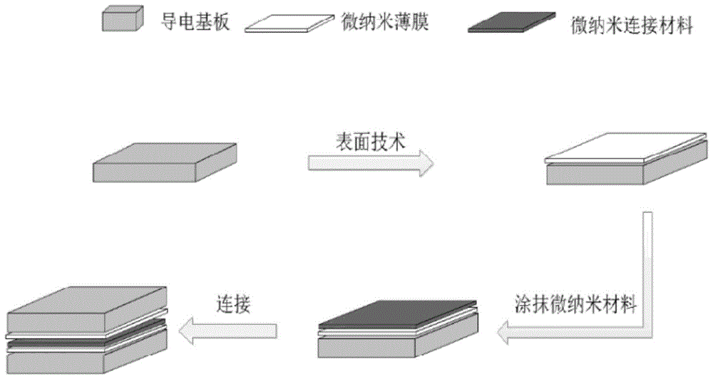
[0018] Specific Embodiment 1: In this embodiment, the method for quickly connecting the activated metal surface and the micro-nano connecting material at a low temperature is carried out according to the following steps:
[0019] 1. Select the substrate material to be surface activated;
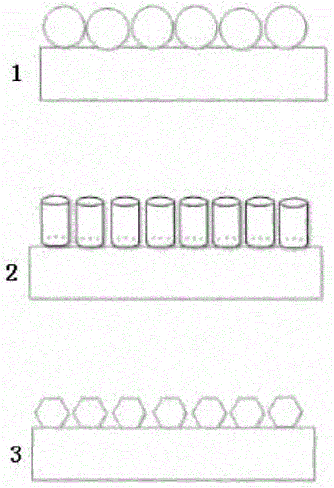
[0020] 2. Use surface technology to prepare metal micro-nano structures on the surface of the substrate, and then cover the metal micro-nano structures with a gold layer, and control the thickness of the gold layer to 0.05 μm to 0.10 μm;
[0021] 3. Select micro-nano connecting materials with a diameter of 10nm-20μm as solder;
[0022] 4. Apply micro-nano connecting material on the surface of the substrate treated in step 2, then take the substrate treated in step 2, and bond the two substrates, thereby completing the vertical interconnection of the two substrate stacks.
[0023] The beneficial effect of this implementation mode:
[0024] The advantages and positive effects of this embodime...
specific Embodiment approach 2
[0025] Embodiment 2: The difference between this embodiment and Embodiment 1 is that the substrate material in step 1 is copper, iron, copper alloy, iron alloy or silicon wafer. Others are the same as in the first embodiment.
specific Embodiment approach 3
[0026] Specific embodiment three: the difference between this embodiment and specific embodiment one or two is: the surface technology described in step two is screen printing, magnetron sputtering, chemical vapor deposition, chemical deposition or template electrodeposition, and control The micro-nano structure has a height of 0.2 μm to 2.0 μm, a particle diameter of 50 nm to 200 nm, and a thickness of 2 μm to 8 μm. Others are the same as in the first or second embodiment.
PUM
| Property | Measurement | Unit |
|---|---|---|
| diameter | aaaaa | aaaaa |
| diameter | aaaaa | aaaaa |
| height | aaaaa | aaaaa |
Abstract
Description
Claims
Application Information

