
LED of novel quantum well structure and method for manufacturing LED

A manufacturing method, quantum well technology, applied in the direction of electrical components, circuits, semiconductor devices, etc., can solve the problem of difficult to obtain free hole concentration and mobility epitaxial wafers, hole injection and transport obstacles, low mobility of effective mass, etc. problem, to achieve the effect of weakening the efficientdroop effect, increasing the luminous power, and increasing the probability of matching

Inactive Publication Date: 2014-08-13
GUANGDONG DELI PHOTOELECTRIC
View PDF5 Cites 20 Cited by
  • Summary
  • Abstract
  • Description
  • Claims
  • Application Information

AI Technical Summary

Problems solved by technology

The hole has a large effective mass and low mobility, and the electron blocking layer and the quantum well barrier layer also hinder the injection and transport of the hole. In GaN-based materials, due to the Mg dopant has With higher activation energy, it is difficult to obtain epitaxial wafers with higher free hole concentration and mobility, so the hole injection efficiency will be greatly reduced

Method used

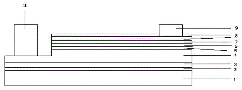

Image

  • LED of novel quantum well structure and method for manufacturing LED
  • LED of novel quantum well structure and method for manufacturing LED
  • LED of novel quantum well structure and method for manufacturing LED

Examples


Embodiment 1

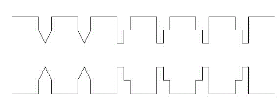
[0026] Embodiment 1: quantum well structure such as figure 2 As shown, there are seven barriers and six wells co-grown in the thickness direction from left to right. The first and second quantum wells both have an inner slope structure and are graded composition quantum wells. The third, fourth, and Both the fifth and sixth quantum wells have internal step structures, which are step-type component quantum wells.

Embodiment 2

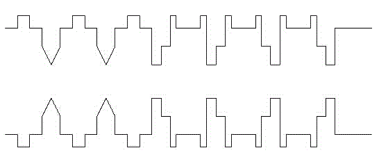
[0027] Embodiment 2: quantum well structure such as image 3 As shown, on the basis of Example 1, the barriers of the first, second and third quantum wells all have outwardly convex structures, which are convex group barriers, and the fourth, fifth and sixth quantum wells All have an inward concave structure, which is a barrier for concave groups.

Embodiment 3

[0028] Embodiment 3: quantum well structure such as Figure 4 As shown, there are seven barriers and six wells co-grown in the thickness direction from left to right, and the first, second, third, and fourth quantum wells all have inner slope structures, which are graded composition quantum wells. The fifth and sixth quantum wells are all thin inner step structures, which are δ-type component quantum wells.


PUM

PropertyMeasurementUnit
Thicknessaaaaaaaaaa

Abstract

The invention discloses an LED of a novel quantum well structure. The LED comprises a substrate and an epitaxial layer structure formed on the substrate. The LED is characterized in that the epitaxial layer structure comprises luminous-layer multiple quantum wells, and well layers and barrier layers of the luminous-layer multiple quantum wells are respectively formed by combining one or more of single-component InGaN, gradually-deformed component InGaN, step-shaped component InGaN, concave component InGaN, convex component InGaN and delta type component InGaN, wherein the In content and the Al content of the mixed quantum wells are achieved by changing parameters such as the In source flow, the Al source flow, growth temperature and growth pressure. According to the structure of the LED, the polarization effect in the GaN-based LED quantum wells is improved, wave function overlap of electrons and holes is enlarged, and therefore internal quantum efficiency of the LED is promoted, and the efficient droop effect of the LED under a high current is weakened.

Description

technical field [0001] The invention relates to a novel LED production technology, in particular to a novel LED quantum well structure and a manufacturing method thereof. Background technique [0002] Group III nitride semiconductors have been extensively studied in recent years, and have become one of the mainstream materials due to their excellent material properties, and are widely used in light-emitting diodes (LEDs), semiconductor lasers, and solar cells. Group III nitride semiconductor LED is the most promising high-tech lighting source in the 21st century. As a new type of high-efficiency solid light source, it has significant advantages such as energy saving and environmental protection. It will be another leap forward in the history of human lighting after incandescent lamps, fluorescent lamps, and high-pressure gas discharge lamps. However, with the gradual increase of forward current, the quantum efficiency of LED drops sharply, which is commonly referred to as t...

Claims


Application Information

Patent Timeline
IPC IPC(8): H01L33/06H01L33/00
CPCH01L33/0075H01L33/06
Inventor 罗长得叶国光林振贤刘洋
Owner GUANGDONG DELI PHOTOELECTRIC
Learn More