Non-blocking 2 * 2 optical switching node based on embedded type silicon substrate micro-ring resonant cavities

A micro-ring resonator and optical switching node technology, applied in data switching network, optics, nonlinear optics, etc., can solve the problem of increasing switching node power consumption, affecting system power consumption and signal quality, reducing signal quality after switching, etc. question

Inactive Publication Date: 2014-08-13
SHANGHAI JIAO TONG UNIV
View PDF3 Cites 15 Cited by
  • Summary
  • Abstract
  • Description
  • Claims
  • Application Information

AI Technical Summary

Problems solved by technology

In practical applications, too low extinction ratio and too high crosstalk will increase the power consumption of switching nodes and reduce the quality of switched signals
Considering the conditions for large-scale on-chip integrated development, the power consumption and switc...

Method used


Image

  • Non-blocking 2 * 2 optical switching node based on embedded type silicon substrate micro-ring resonant cavities
  • Non-blocking 2 * 2 optical switching node based on embedded type silicon substrate micro-ring resonant cavities
  • Non-blocking 2 * 2 optical switching node based on embedded type silicon substrate micro-ring resonant cavities

Examples


Embodiment 1

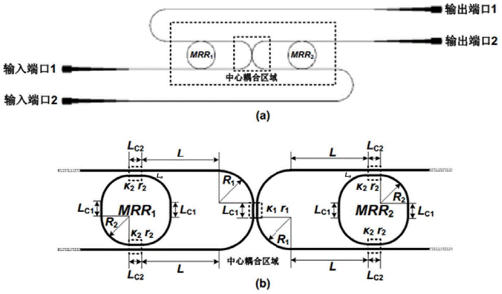
[0024] Such as figure 1 As shown, this embodiment consists of two symmetrically arranged nested silicon-based microring resonators made of silicon-on-insulator wafers. The U-shaped waveguides of the nested silicon-based microring resonators are coupled to each other to form a directional coupler. Since the Benes switching node structure has the least complexity in the non-blocking switching node structure, the design and analysis of the switching node structure is based on this structure.

[0025] The nested silicon-based microring resonator is composed of two U-shaped waveguides in series, wherein: the air gap between the straight waveguide part and the curved waveguide part in the U-shaped waveguide is L a =0.18μm, the length of the coupling part is L c1 =L c2 =7μm, the cross-section of the U-shaped waveguide is 450×220nm2, and the curved waveguide part is an arc-line-arc structure, where the radius of the arc is R 2 = 40 μm, the straight portion L of the U-shaped wavegu...


PUM

PropertyMeasurementUnit
Thicknessaaaaaaaaaa
Thicknessaaaaaaaaaa

Abstract

The invention discloses a non-blocking 2 * 2 optical switching node based on embedded type silicon substrate micro-ring resonant cavities and belongs to the technical field of optical fiber communication. The non-blocking 2 * 2 optical switching node comprises two embedded type silicon substrate micro-ring resonant cavities which are arranged in a central-symmetry mode and are made of silicon wafers on insulators, and the resonant cavities are of an S-shaped structure. Two opposite U-shaped waveguides of the embedded type silicon substrate micro-ring resonant cavities form a directional coupler in a coupling mode. The outer sides of the two U-shaped waveguides are respectively provided with a micro-ring resonator. The optical switching node comprises four input-output switching ports which form two groups. Under crossing and shoot-through states, actually-measured extinction ratios reach 44.7 dB and 38.0 dB respectively, crosstalk values are lowered to -37.5 dB and -45.2 dB respectively, and for 10 Gb/s and 12.5 Gb/s non-return-to-zero (NRZ) signals, an error-code-free node switching function can be achieved.

Description

technical field [0001] The invention relates to a device in the technical field of optical fiber communication, in particular to a non-blocking 2×2 optical switching node based on a nested silicon-based micro-ring resonant cavity. Background technique [0002] With the development of semiconductor technology, the transmission and processing speed of modern communication is constantly increasing. While the ability of multi-core processors to process information has been steadily improving, the interconnection between chips has become a huge limiting factor. The wires that connect chips, boards, and systems will struggle to keep up with Moore's Law. Traditional on-chip interconnection technology is restricted by the physical characteristics of electrical interconnection, and the improvement of physical characteristics such as delay, bandwidth, and power consumption in transmission has become a bottleneck in the improvement of communication capacity. Optical interconnect tech...

Claims


Application Information

Patent Timeline
IPC IPC(8): H04L12/931H04Q11/00G02F1/01
Inventor 潘听吴佳旸杨玉星姜新红曹攀苏翼凯
Owner SHANGHAI JIAO TONG UNIV
Why Eureka
Try Eureka