ITO powder, ITO painting for conductive film and manufacture method for transparent conductive film
A technology of conductive film and powder, which is applied in the field of ITO powder, can solve the problems of performance deterioration, resistance increase of transparent conductive film, and easy generation of voids in ITO micro-powder, so as to achieve the effect of increasing contact area and reducing resistance
- Summary
- Abstract
- Description
- Claims
- Application Information
AI Technical Summary
Problems solved by technology
Method used
Image
Examples
Embodiment
[0052] Hereinafter, examples and comparative examples of the present invention will be described in detail.
[0053]
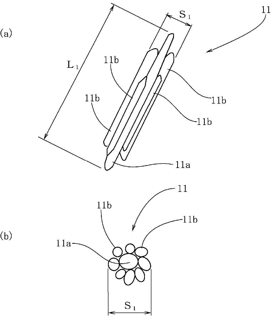
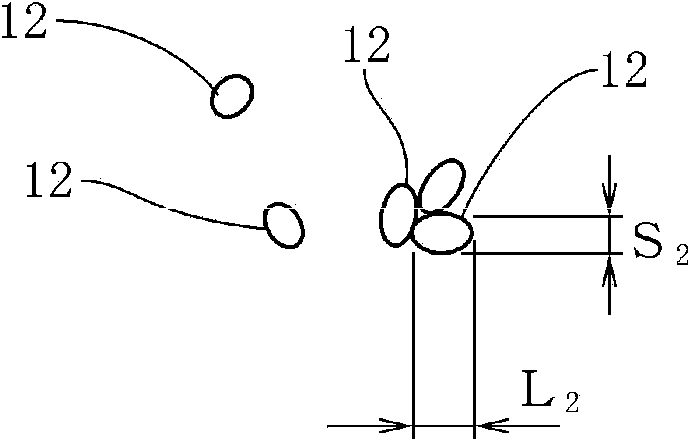
[0054] In order to make the first powder, first weigh an indium chloride aqueous solution (InCl 3 ) 100g and tin chloride (SnCl 4 ·5H 2 O) 6.3g was dissolved in 2000ml of pure water to prepare a mixed solution of indium chloride and tin chloride. The concentration of tin in this mixed solution was adjusted so that the molar ratio of Sn / In was 0.10. This mixed solution of indium chloride and tin chloride was heated to 60° C., and 29% by mass of ammonia water was gradually added over 160 minutes to prepare a tin-containing indium hydroxide suspension. Next, aqueous ammonia was added to the suspension, and ultrasonic waves of 34 kHz were applied to the suspension to prevent aggregation and produce aggregates of polycrystalline ITO particles while precipitation was being produced. The suspension containing tin-indium hydroxide was collected by filtration and...
Embodiment 2
[0064] Except for the average major axis diameter L of the first powder 1 Except for 200 nm, it carried out similarly to Example 1, and produced the transparent conductive film. This transparent conductive film was referred to as Example 2.
Embodiment 3
[0066] In addition to changing the ultrasonic irradiation of the suspension so that the average long-axis diameter L of the first powder 1 A transparent conductive film was produced in the same manner as in Example 1 except that the total reaction time was 3000 nm. This transparent conductive film was referred to as Example 3.
PUM
| Property | Measurement | Unit |
|---|---|---|
| Resistivity | aaaaa | aaaaa |
| Surface resistance | aaaaa | aaaaa |
| Surface resistance | aaaaa | aaaaa |
Abstract
Description
Claims
Application Information


