Manufacturing method of groove power device

A technology of power devices and manufacturing methods, applied in semiconductor/solid-state device manufacturing, semiconductor devices, electrical components, etc., can solve the problems of thin gate oxide layer 103 damage, lower device yield, complex manufacturing process, etc., to increase the difficulty of the process , Simplified manufacturing process, low cost effect

Inactive Publication Date: 2014-08-27
SUZHOU ORIENTAL SEMICONDUCTOR CO LTD
View PDF3 Cites 2 Cited by
  • Summary
  • Abstract
  • Description
  • Claims
  • Application Information

AI Technical Summary

Problems solved by technology

[0004] In the manufacturing method of the above-mentioned trench type MOS transistor device, when the thin gate oxide layer 103 is oxidized, an oxide layer will be formed on the surface of the polysilicon sacrificial dielectric layer, thereby blocking the connection between the polysilicon sacrificial dielectric layer 102 and the external electrodes. To affect this connection, it is necessary to etch off the oxide layer on the surface of the polysilicon sacrificial dielectric layer, but the thin gate oxide layer 103 will be damaged during etching, so it is necessary to etch away the polysilicon sacrificial dielectric layer 102 and the thin gate oxide layer at the same time. Oxide layer 103, and then re-oxidize the gate oxide layer and deposit the polysilicon gate, which makes the manufacturing process of the device very complicated, not only the manufacturing cost is high, but also reduces the yield of the device

Method used


Image

  • Manufacturing method of groove power device
  • Manufacturing method of groove power device
  • Manufacturing method of groove power device

Examples


Embodiment Construction

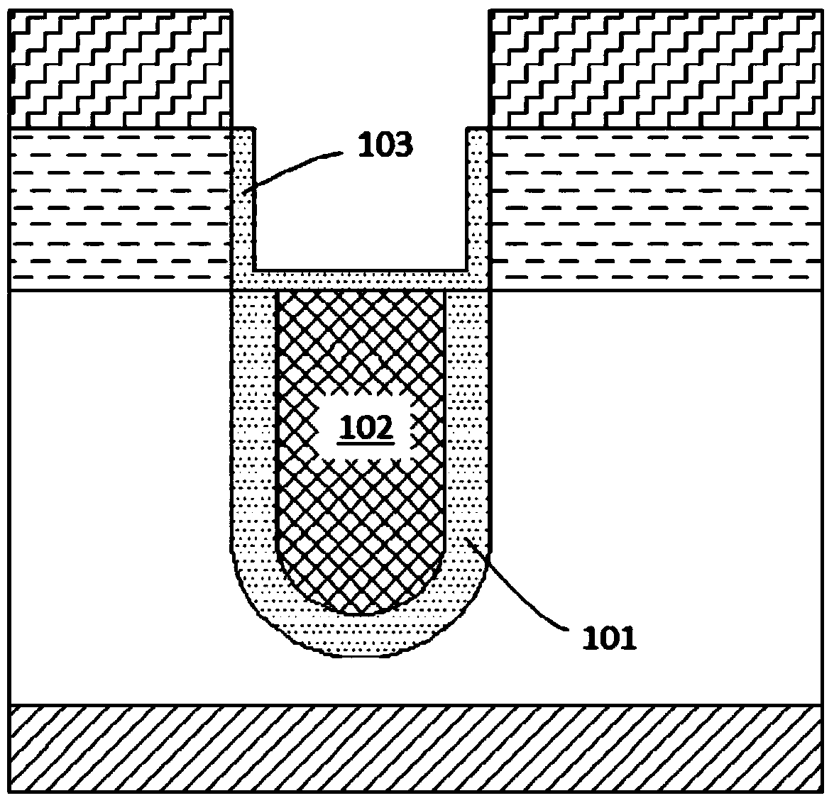
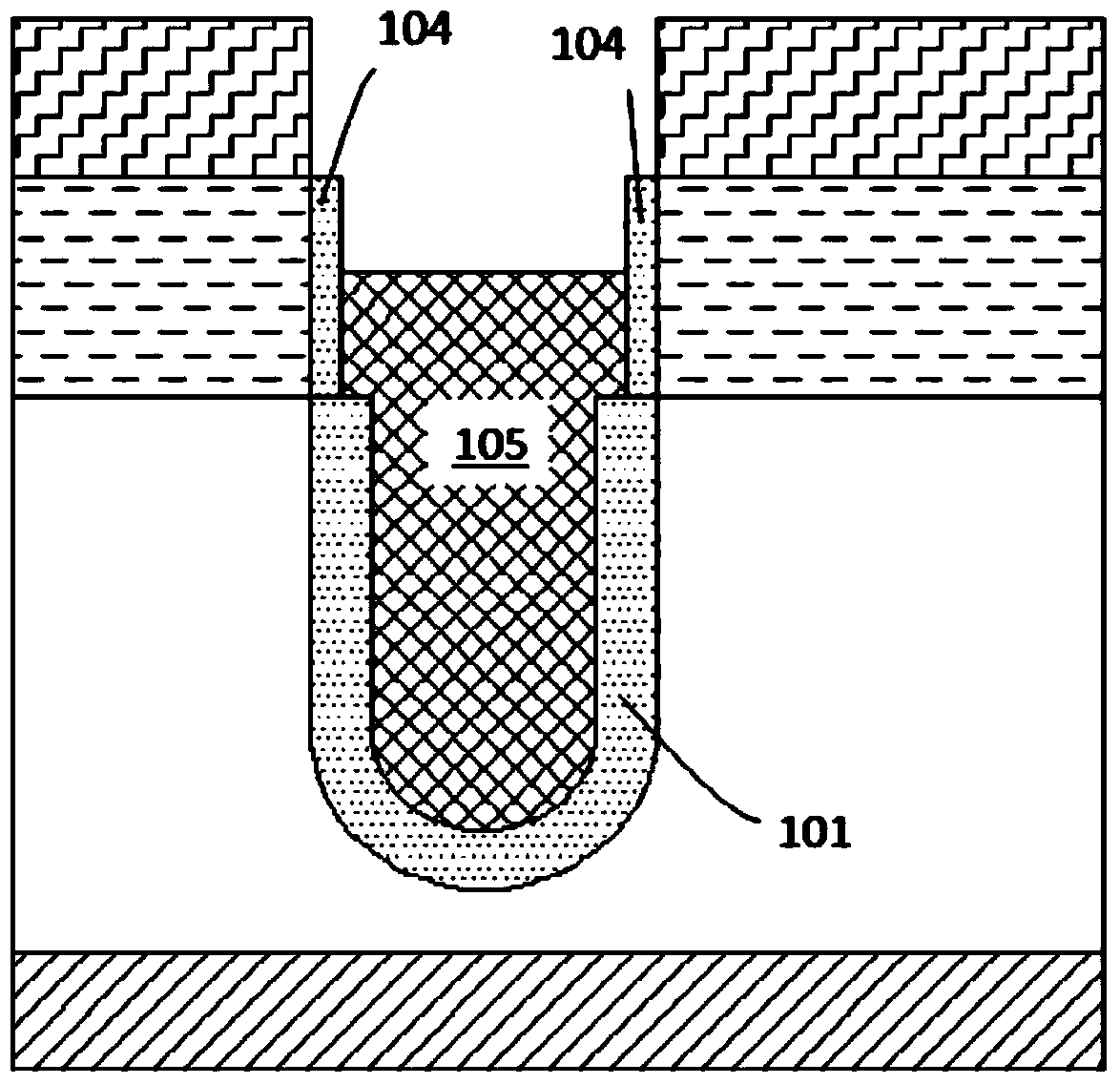
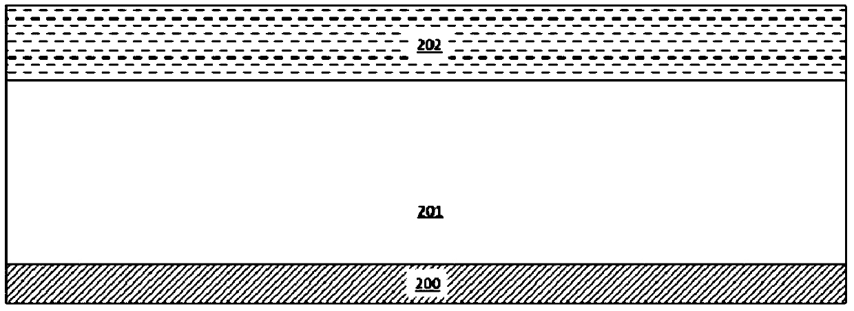
[0040] In order to clearly illustrate the specific implementation of the present invention, the figures listed in the accompanying drawings of the description enlarge the thickness of the layers and regions described in the present invention, and the size of the figures shown does not represent the actual size; the drawings are schematic , should not limit the scope of the present invention. The embodiments listed in the description should not be limited to the specific shapes of the regions shown in the drawings, but include the obtained shapes such as deviations caused by manufacturing, etc., and the curves obtained by etching usually have curved or rounded characteristics, but All are represented by rectangles in the embodiments of the present invention; meanwhile, in the following description, the term semiconductor substrate used can be understood to include the semiconductor wafer being processed and other thin film layers prepared thereon.

[0041] The specific implemen...


PUM

PropertyMeasurementUnit
thicknessaaaaaaaaaa
thicknessaaaaaaaaaa
thicknessaaaaaaaaaa

Abstract

The invention belongs to the technical field of manufacturing of semiconductor power devices, and particularly relates to a manufacturing method of a groove power device. The manufacturing method includes the steps that after a field oxide layer is formed in a U-shaped groove of the device, photoresist is adopted as a sacrificial dielectric layer, the developed photoresist is reserved only in the U-shaped groove by controlling the exposure time and the development time of the photoresist, then the exposed portions of the field oxide layer are etched away, then the photoresist is stripped, then a gate oxide layer is oxidized, a polycrystalline silicon grid electrode is deposited, and finally source electrode metal making contact with a source area and a channel doping area is formed. The manufacturing method has the advantages of being simple and reliable in technical process, easy to control and the like, the production cost of the groove power device can be lowered, and yield of the groove power device can be improved.

Description

technical field [0001] The invention belongs to the technical field of manufacturing semiconductor power devices, in particular to a method for manufacturing trench power devices. Background technique [0002] With the continuous development of modern microelectronics technology, power MOS transistors have high input impedance, low loss, fast switching speed, no secondary breakdown, wide safe working area, good dynamic performance, and easy coupling with the front electrode to achieve high current. With the advantages of high efficiency and high conversion efficiency, it has gradually replaced bipolar devices and become the mainstream of power device development today. Known power devices mainly include planar diffusion MOS transistors and trench MOS transistors. Taking the trench type MOS transistor as an example, because the device adopts a vertical channel type structure, its area is much smaller than that of the planar diffusion type MOS transistor, so its current densi...

Claims


Application Information

Patent Timeline
Patent Type & Authority Applications(China)
IPC IPC(8): H01L21/336
CPCH01L29/66068H01L21/28008H01L29/401H01L29/66666
Inventor 刘磊苗跃王鹏飞龚轶
Owner SUZHOU ORIENTAL SEMICONDUCTOR CO LTD
Why Eureka
Try Eureka