Low-modulus conductive adhesive for semiconductor chip packaging
A chip packaging, low modulus technology, applied in the field of conductive adhesive, can solve problems such as large modulus, and achieve the effect of small modulus and good electrical conductivity
- Summary
- Abstract
- Description
- Claims
- Application Information
AI Technical Summary
Problems solved by technology
Method used
Image

Examples
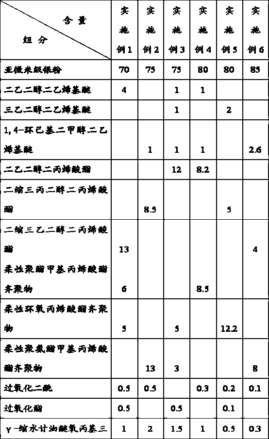
Embodiment 1
[0028] At room temperature, according to the components specified in Example 1 in the following table, diethylene glycol divinyl ether, triethylene glycol diacrylate, flexible polyester methacrylate oligomer and flexible Mix the epoxy acrylate oligomer at room temperature for 30 minutes until uniform, then add diacyl peroxide, peroxide ester, γ-glycidyl etheroxypropyl trimethoxysilane, γ-methacryloxypropyl trimethyl Oxysilane and γ-methacryloxypropyltriisopropoxysilane, mixed at room temperature for 30 minutes to form a homogeneous mixture, added submicron silver powder, applied vacuum at room temperature and mixed at low speed for 30 minutes to prepare a conductive adhesive .
Embodiment 2
[0030] At room temperature, according to the components specified in Example 2 in the table below, 1,4-cyclohexyldimethanol divinyl ether, tripropylene glycol diacrylate and flexible polyurethane methacrylate oligomer were prepared at room temperature Mix for 30 minutes until uniform, then add diacyl peroxide, γ-glycidyloxypropyltrimethoxysilane and γ-methacryloxypropyltrimethoxysilane, and mix for 30 minutes at room temperature to form a homogeneous mixture , add sub-micron silver powder, apply vacuum and mix at low speed for 60 minutes at room temperature to prepare conductive adhesive.
Embodiment 3
[0032] At room temperature, according to the components specified in Example 3 in the table below, diethylene glycol divinyl ether, triethylene glycol divinyl ether, 1,4-cyclohexyldimethanol divinyl ether, Diethylene glycol diacrylate, flexible epoxy acrylate oligomer and flexible polyurethane methacrylate oligomer were mixed at room temperature for 30 minutes until uniform, then added peroxide, γ-glycidyl ether oxypropyl trimethoxy Base silane and γ-methacryloxypropyl triisopropoxysilane, mix at room temperature for 30 minutes to form a homogeneous mixture, add submicron silver powder, apply vacuum at room temperature and mix at low speed for 60 minutes to prepare the conductive adhesive.
PUM
 Abstract
Description
Claims
Application Information
 - R&D Engineer
- R&D Manager
- IP Professional
- Industry Leading Data Capabilities
- Powerful AI technology
- Patent DNA Extraction
Browse by: Latest US Patents, China's latest patents, Technical Efficacy Thesaurus, Application Domain, Technology Topic.
© 2024 PatSnap. All rights reserved.Legal|Privacy policy|Modern Slavery Act Transparency Statement|Sitemap