Method for protecting epitaxial growth interface in selection region

A technology of selective area epitaxy and interface protection, applied in the direction of crystal growth, single crystal growth, chemical instruments and methods, etc., can solve the problems of high carrier surface density, damage to the growth interface of the selected area, failure to etch the dielectric layer cleanly, etc. , to achieve the effect of improving crystal quality

Inactive Publication Date: 2014-09-03
SUN YAT SEN UNIV
View PDF12 Cites 0 Cited by
  • Summary
  • Abstract
  • Description
  • Claims
  • Application Information

AI Technical Summary

Problems solved by technology

However, the following problems will be encountered in the process of this masking process: First, the dielectric layer is often not etched clean when the dielectric layer is removed by the etching process, and there will be some residues at the interface of the selected growth area, making the growth interface rough and difficult to nucleate and grow
The second is that when the dielectric layer is deposited in the region where selective growth is required, the elements in the dielectric layer will be injected into the substrate to form unintentional doping on the substrate, which will affect the performance of the growth material, thereby affecting the performance of the device
For example, SiO is often used for selective area epitaxial growth of III / V compound semiconductor materials. 2 as mask material, while SiO 2 When the PECVD method is used for deposition and growth, due to the high temperature environment, Si and O elements may diffuse to the III / V group substrate to form donor-like doping, which will make the heterostructure of the secondary epitaxial growth appear compared with the primary epitaxial growth. The phenomenon that the carrier surface density is too high and the electron mobility decreases will directly affect the performance of the prepared electronic device
It can be seen that the traditional selective region growth mask layer formation method will damage the selective region growth interface

Method used


Image

  • Method for protecting epitaxial growth interface in selection region
  • Method for protecting epitaxial growth interface in selection region
  • Method for protecting epitaxial growth interface in selection region

Examples


Embodiment Construction

[0033]The accompanying drawings are for illustrative purposes only, and should not be construed as limitations on this patent; in order to better illustrate this embodiment, certain components in the accompanying drawings will be omitted, enlarged or reduced, and do not represent the size of the actual product; for those skilled in the art It is understandable that some well-known structures and descriptions thereof may be omitted in the drawings. The positional relationship described in the drawings is for illustrative purposes only, and should not be construed as a limitation on this patent.

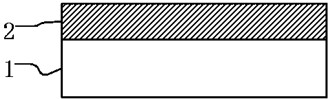
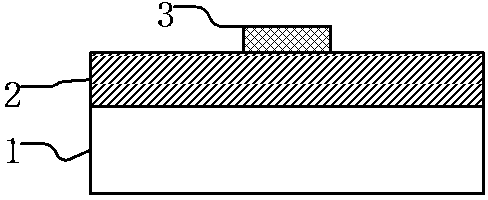
[0034] like Image 6 As shown, it is a schematic diagram of the structure of the AlGaN / GaN selective area epitaxial material prepared in this embodiment, which involves a selective area epitaxial growth interface protection method, and its detailed process steps include the following:

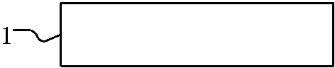
[0035] 1. If Figure 7 As shown, a substrate 1 requiring epitaxial growth is provided; in this emb...


PUM


Abstract

The invention provides a semiconductor process method and in particular relates to a method for protecting an epitaxial growth interface in a selection region. The method comprises the following steps: providing a substrate with the need of epitaxial growth, partially covering a photoresist protective layer on the substrate, and further depositing a dielectric layer on the photoresist protective layer to serve as a mask layer; removing the photoresist protective layer and the dielectric layer on the photoresist protective layer by adopting a photoresist lift off process, and patterning the mask layer; and finally, performing epitaxial growth on an area which is not masked. The process is simple, and the problem that the growth interface is easily damaged in the process of manufacturing the mask layer in the traditional photoetching and eroding method can be well solved.

Description

technical field [0001] The present invention relates to the technical field of semiconductor epitaxial technology, and more specifically, relates to a method for protecting a selective region epitaxial growth interface. Background technique [0002] Selected area growth (SAG) is widely used in semiconductor epitaxial growth and device manufacturing. Selected area growth techniques can be used to control crystal quality, the most common is the use of selective area epitaxy to achieve lateral epitaxy (ELO), which reduces the dislocation density penetrating to the surface of the material (see Kazumasa Hiramatsu, Epitaxial lateral overgrowth techniques used in group III nitride epitaxy, J. Phys.: Condens. Matter 13 (2001), 6961–6975). In addition to controlling the crystal quality, the selective area epitaxy technology is also used in the preparation of special structures, generally for the realization of special structures required for devices in planar processes, such as the...

Claims


Application Information

Patent Timeline
Patent Type & Authority Applications(China)
IPC IPC(8): C30B25/04C30B23/04
Inventor 刘扬周德秋杨帆倪毅强
Owner SUN YAT SEN UNIV
Why Eureka
Try Eureka