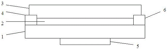
a mos 2 thin film transistor

A thin-film transistor and thin-film technology, which is applied in the direction of transistors, semiconductor devices, electrical components, etc., can solve the problems of increasing power consumption, increasing light intensity of light sources, and low mobility of amorphous silicon materials, so as to increase the pixel aperture ratio and increase light Transmittance, effect of improving display quality

Inactive Publication Date: 2017-01-25
NANCHANG UNIV
View PDF2 Cites 0 Cited by
  • Summary
  • Abstract
  • Description
  • Claims
  • Application Information

AI Technical Summary

Problems solved by technology

The most widely used thin-film transistors in liquid crystal displays are hydrogenated amorphous silicon thin-film transistors, but the mobility of amorphous silicon materials is low, and the drain current is small, which cannot meet the requirements of high-speed and high-brightness displays, and amorphous silicon materials are opaque. , it will occupy a certain area in the pixel and reduce the pixel aperture ratio
Since light cannot pass through all pixels, in order to obtain sufficient brightness, it is necessary to increase the light intensity of the light source, thereby increasing power consumption

Method used


Image

  • a mos  <sub>2</sub> thin film transistor
  • a mos  <sub>2</sub> thin film transistor
  • a mos  <sub>2</sub> thin film transistor

Examples


Embodiment 1

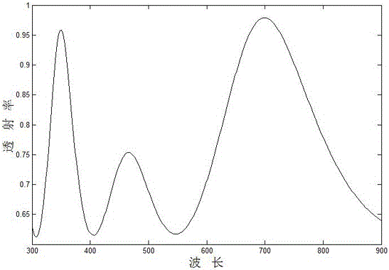
[0024] MoS 2 The base layer of thin film transistors is SiO 2 Refractive index , the gate dielectric layer is HfO 2 Refractive index , according to the requirement of maximum red light transmittance, design SiO 2 layer and HfO 2 The layer thicknesses are and ,in The wavelength of red light is taken as 700nm, where , , so SiO 2 layer and HfO 2 The thicknesses of the layers are designed to be 239 nm and 140 nm, respectively.

Embodiment 2

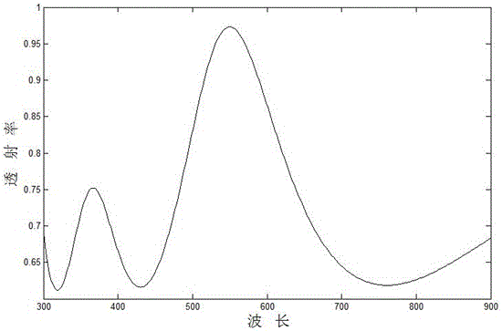
[0026] MoS 2 The base layer of thin film transistors is SiO 2 Refractive index , the gate dielectric layer is HfO 2 Refractive index , according to the requirement of maximum green light transmittance, design SiO 2 layer and HfO 2 The layer thicknesses are and ,in The wavelength of green light is taken as 550nm, where , , so SiO 2 layer and HfO 2 The thicknesses of the layers are designed to be 188nm and 110nm, respectively.

Embodiment 3

[0028] MoS 2 The base layer of thin film transistors is SiO 2 Refractive index , the gate dielectric layer is HfO 2 Refractive index , according to the requirement of maximum blue light transmittance, design SiO 2 layer and HfO 2 The layer thicknesses are and ,in The wavelength of blue light is taken as 480nm, where , , so SiO 2 layer and HfO 2 The thicknesses of the layers are designed to be 164nm and 96nm, respectively.


PUM


Abstract

The invention discloses a MoS2 thin-film transistor which is characterized in that: the MoS2 thin-film transistor is composed of a lower substrate layer, a middle channel layer and an upper gate dielectric layer; the channel layer is a single-layer MoS2 film; the gate dielectric layer is an HfO2 layer with a specific thickness. According to the MoS2 thin-film transistor, transmissivity of the transistor can be increased through changing the thicknesses of the substrate layer and the gate dielectric layer, thereby obtaining the MoS2 thin-film transistor with an ultra high transmissivity, improving aperture ratio of pixels in a thin-film transistor liquid crystal display, improving displaying quality and reducing power consumption.

Description

technical field [0001] The invention relates to a thin film transistor structure, in particular to a controllable high transmittance MoS 2 A thin film transistor structure belongs to the technical field of thin film transistors. Background technique [0002] In the field of display, liquid crystal display (LCD) is the most widely used. The introduction of thin-film transistor switching elements in LCD pixels can greatly improve the performance of display devices. Thin-film transistor liquid crystal display has become the mainstream of display technology. The most widely used thin-film transistors in liquid crystal displays are hydrogenated amorphous silicon thin-film transistors, but the mobility of amorphous silicon materials is low, and the drain current is small, which cannot meet the requirements of high-speed and high-brightness displays, and amorphous silicon materials are opaque. , it will occupy a certain area in the pixel and reduce the pixel aperture ratio. Since...

Claims


Application Information

Patent Timeline
Patent Type & Authority Patents(China)
IPC IPC(8): H01L29/786H01L29/12
CPCH01L29/0657H01L29/24H01L29/78603H01L2029/42388
Inventor 杨方方刘江涛刘念华
Owner NANCHANG UNIV
Why Eureka
Try Eureka