

Method of using thin plates of same kind of material to prepare rectangular grating structure
A technology of rectangular gratings and material thin plates, applied in diffraction gratings, cold cathode manufacturing, electrode system manufacturing, etc., can solve the problems of large side roughness, expensive equipment, small grating groove aspect ratio, etc., and achieve smooth and steep sides, The effect of large aspect ratio
- Summary
- Abstract
- Description
- Claims
- Application Information
AI Technical Summary
Problems solved by technology
Method used
Image

Examples
Embodiment 1
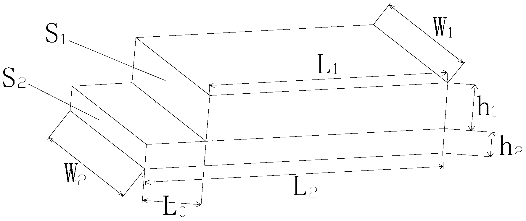
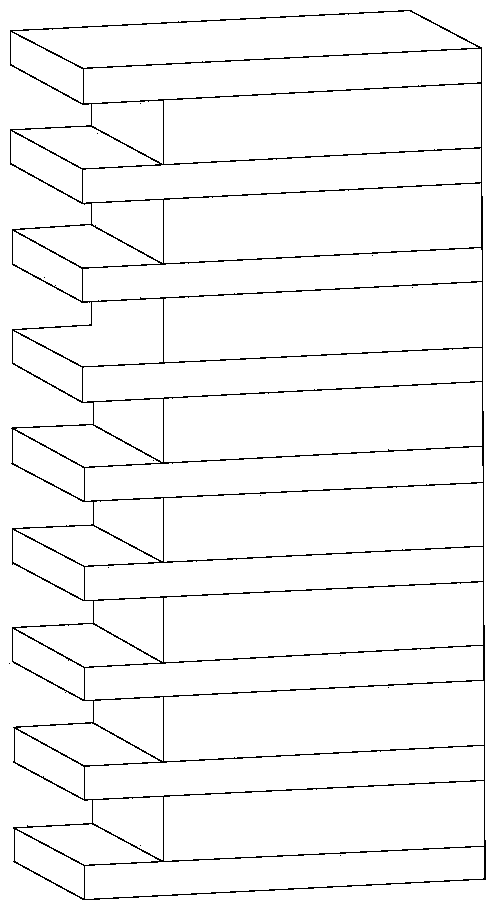
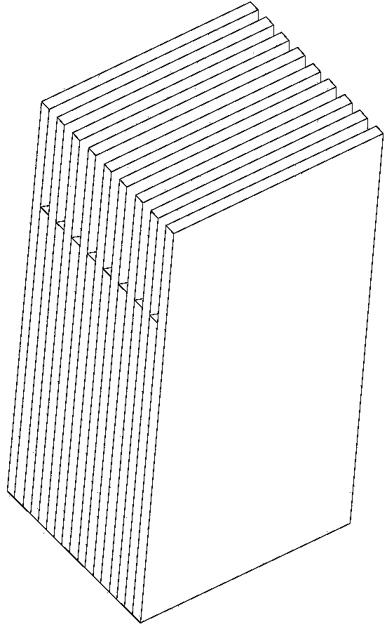
[0021] First prepare the thickness h 1 、h 2 Two types of veneer, the surface of the veneer is sanded to make it smooth. Then, the two kinds of thin plates are cross-stacked, and one of the end faces of the stacked structure meets the following requirements: 1) The distance between adjacent thin plates at this end is equal; 2) The thickness of the alternate thin plates is the same, and the side faces at this end are on the same 3) The side of each thin plate at the end face is perpendicular to the upper and lower surfaces of the thin plate. Finally, the structure is made into a single piece by resistance welding or other processes. In this way, a grating structure is formed on the end face, where the period l of the grating is determined by the thickness of the two thin plates (ie l = h 1 + h 2 ), the depth of the grating groove is determined by the distance between the adjacent thin plates at the end, and the width of the grating groove is determined by the thickness of th...
Embodiment 2
[0035] To fabricate an oxygen-free copper grating that can be used as a slow-wave system for diffractive radiation vacuum electronic devices, the period length l of the grating is required to be 0.1 mm, the groove width is 0.05 mm, and the depth is 5 mm.
[0036] Step 1. Material preparation
[0037] Prepared by mechanical processing or purchased commercially, obtain oxygen-free copper sheets with a thickness of 0.05 mm, and then process these sheets into two cuboids with a width of 20 mm×10 mm×0.05 mm and a thickness of 15 mm×10 mm×0.05 mm by cutting A and B, the surface roughness of these cuboids is required to be less than 50nm.
[0038] Step 2. Stacking of plates
[0039] When stacking, two boards with different lengths should be stacked alternately, and the short sides and long sides are parallel to each other, and the following principles should be followed:
[0040] 1) The length of the interphase plates is the same, and the long and wide sides of the interphase p...
PUM
| Property | Measurement | Unit |
|---|---|---|
| Slot width | aaaaa | aaaaa |
| Depth | aaaaa | aaaaa |
| Surface roughness | aaaaa | aaaaa |
Abstract
Description
Claims
Application Information