Millimeter wave chip carrier based on high temperature co-fired ceramic and manufacturing method thereof

A technology of high-temperature co-fired ceramics and chip casings, which is applied in the manufacture of semiconductor/solid-state devices, electrical components, and electrical solid-state devices. It can solve the problems of high processing accuracy, limited application, high dielectric constant and dielectric loss, and achieve good isolation , to avoid the effect of resonance

Inactive Publication Date: 2014-09-17
NO 55 INST CHINA ELECTRONIC SCI & TECHNOLOGYGROUP CO LTD
View PDF3 Cites 19 Cited by
  • Summary
  • Abstract
  • Description
  • Claims
  • Application Information

AI Technical Summary

Problems solved by technology

However, due to the fact that the material properties of HTCC are slightly worse than those of LTCC materials, alumina ceramic materials have relatively higher dielectric constant and dielectric loss than LTCC ceramics, and the processing accuracy of domestic HTCC is not as high as that of LTCC.
These limit the application of HTCC in millimeter wave chip housings

Method used


Image

  • Millimeter wave chip carrier based on high temperature co-fired ceramic and manufacturing method thereof
  • Millimeter wave chip carrier based on high temperature co-fired ceramic and manufacturing method thereof
  • Millimeter wave chip carrier based on high temperature co-fired ceramic and manufacturing method thereof

Examples


Embodiment Construction

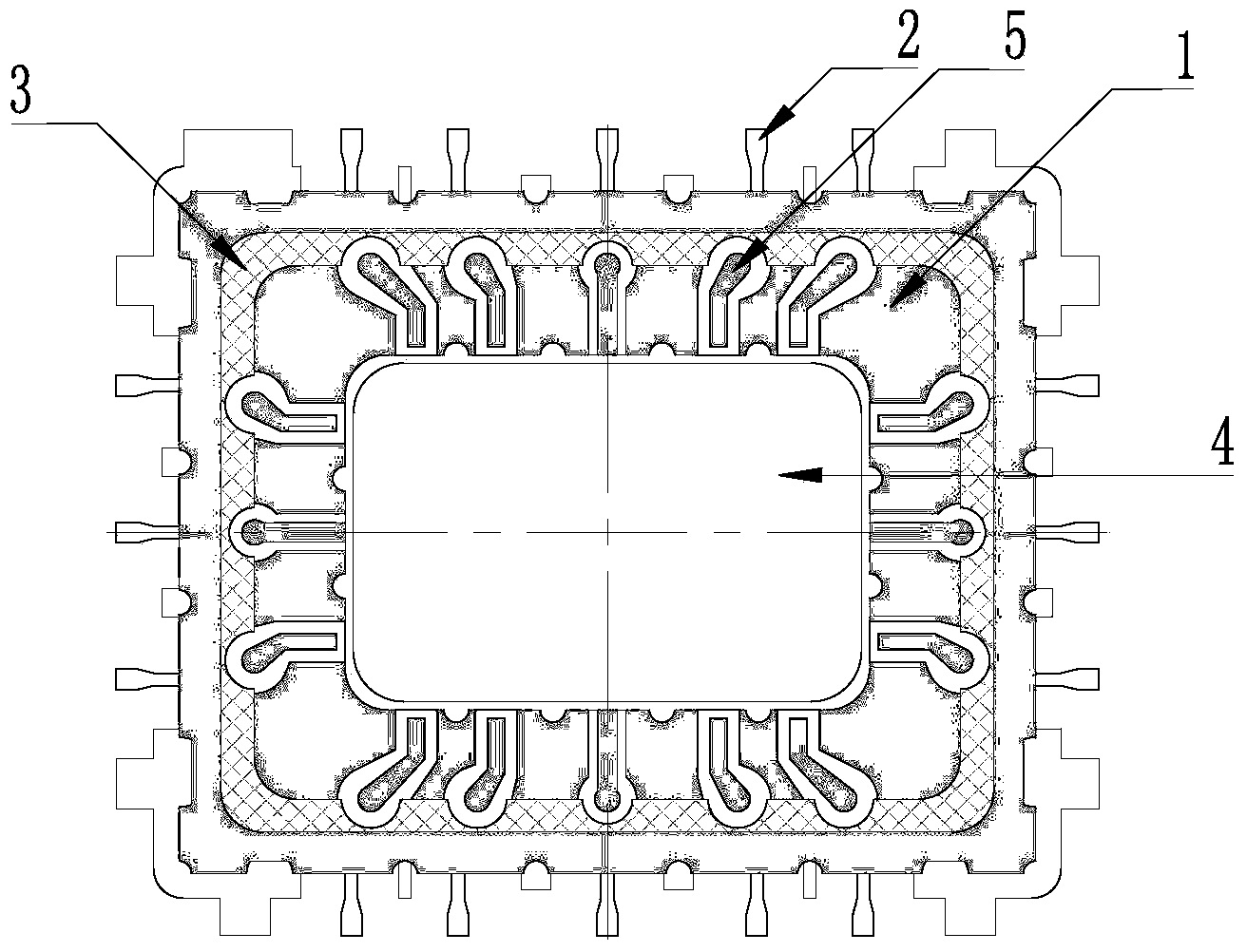
[0027] First refer to figure 1 and figure 2 The structure and outline drawing of the product, the molybdenum-copper gasket with the outline size of 6.05mm*4.10mm*0.35mm, the molybdenum-copper base of 7.13mm*5.18mm*0.15mm and the possible cutting leads. Routine cleaning is carried out to the above-mentioned metal parts, and they are used after nickel plating.

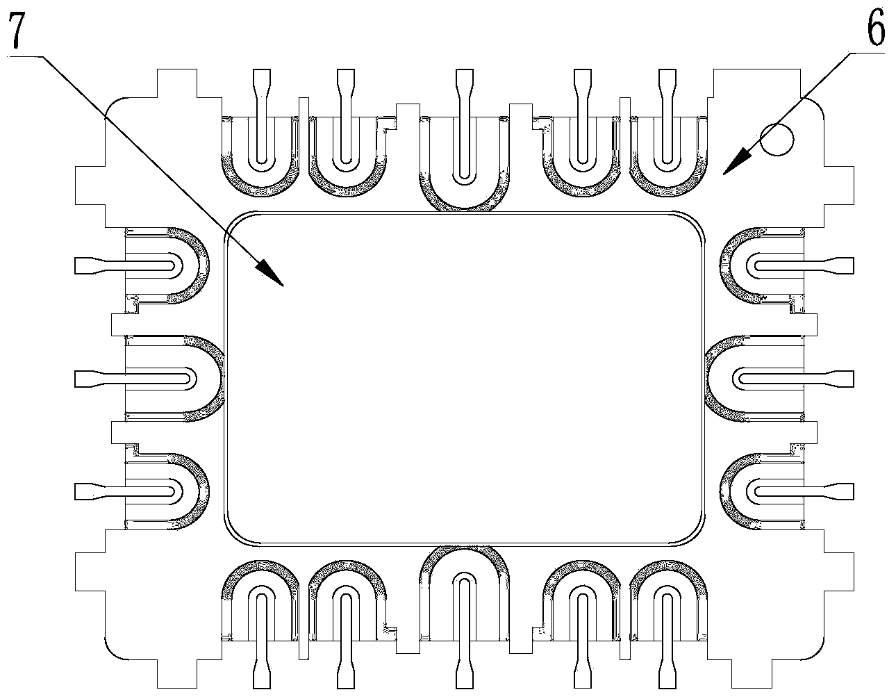
[0028] Second, follow the Figure 5 In the HTCC process shown, the taped raw ceramic tape made of special low-loss ceramic material is used to produce alumina ceramics with a size of 10.21mm*8.25mm*0.5mm, and the internal wiring meets the requirements, and it is nickel-plated for use.

[0029] then follow figure 1 , 2 As shown, the nickel-plated Kovar lead and the molybdenum-copper base are welded to the back of the ceramic part by Ag-Cu solder at a high temperature of about 800 ° C, and then the molybdenum-copper gasket is welded to the front side under the same conditions. in the lumen.

[0030] The above-menti...


PUM

PropertyMeasurementUnit
Sizeaaaaaaaaaa

Abstract

The invention discloses a millimeter wave chip carrier based on high temperature co-fired ceramic and a manufacturing method of the millimeter wave chip carrier. On the basis of a ceramic piece formed by the high temperature co-fired ceramic, commercial molybdenum copper is adopted as a brazing base and a gasket. The surface-mounting type carrier is formed. The millimeter wave chip carrier and the manufacturing method have the advantages that a coplanar waveguide and similar coaxial signal transmission structure is utilized, and the good microwave performance of millimeter waves can be achieved. The heat dissipation capacity, air tightness and long-time reliability of the carrier manufactured according to a technological path and the method can meet the packaging requirement for a Ka waveband device.

Description

technical field [0001] The invention relates to a millimeter wave chip shell and a manufacturing method thereof, in particular to a millimeter wave chip shell based on high temperature co-fired ceramics and a manufacturing method thereof. Background technique [0002] At present, low-temperature co-fired ceramics (LTCC, Low-temperature co-fired ceramic) is a material technology for electronic assembly and packaging that has emerged in recent years. It is one of the preferred methods of modularization and modularization, and is widely used in the manufacture of packaging substrates for microelectronic circuits or modules in the low-frequency to millimeter-wave frequency band. LTCC was developed by Hughes in 1982. The corresponding package substrate processing method is: LTCC (a mixed material made of ceramic powder and glass phase material) is made into a green ceramic tape with precise thickness and density by casting process. The required horizontal and vertical electrical...

Claims


Application Information

Patent Timeline
IPC IPC(8): H01L23/055H01L21/48
Inventor 李永彬庞学满郭玉红陈寰贝程凯
Owner NO 55 INST CHINA ELECTRONIC SCI & TECHNOLOGYGROUP CO LTD
Why Eureka
Try Eureka