Method for preparing micro intercommunicated hole structure transmission electron microscope sample

A technology of transmission electron microscope samples and interconnecting through holes, which is applied in the preparation of test samples, etc., can solve the problems of complicated operation process, easy introduction of pollution, expensive equipment, etc., and achieves simple process flow, no ion pollution, and convenient operation. Effect

Inactive Publication Date: 2014-10-01
INST OF METAL RESEARCH - CHINESE ACAD OF SCI
View PDF4 Cites 13 Cited by
  • Summary
  • Abstract
  • Description
  • Claims
  • Application Information

AI Technical Summary

Problems solved by technology

[0004] The purpose of the present invention is to overcome the shortcomings of expensive equipment, high cost, complicated operation process, and easy introduction of pollution when preparing the transmission electron microscope sample of the through-hole structure sample by the focused ion beam cutting method, and to provide a micro-interconnected through-hole structure transmission electron microscope. The sample preparation method can realize the fine characterization of the microstructure of each interface layer at any hole depth position (such as the surface, upper, middle, lower or bottom) of the through-hole structure sample

Method used


Image

  • Method for preparing micro intercommunicated hole structure transmission electron microscope sample
  • Method for preparing micro intercommunicated hole structure transmission electron microscope sample
  • Method for preparing micro intercommunicated hole structure transmission electron microscope sample

Examples


Embodiment 1

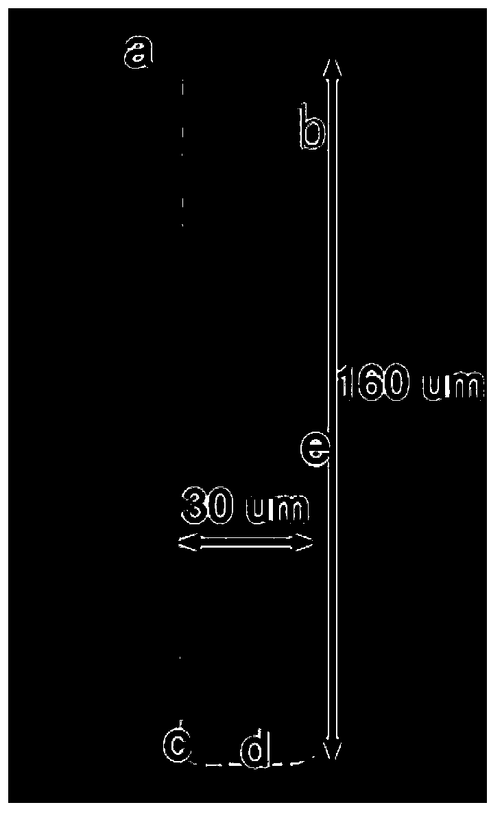
[0041] (1) The TSV through hole is a blind hole, and the size of the through hole is: 30 μm in diameter and 160 μm in depth.

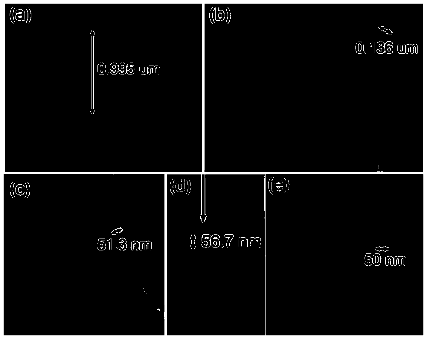
[0042] (2) The TEM sample preparation of the surface position of the TSV, the upper surface of two samples of the same size are directly bonded to make a cross-sectional sample; among them, the adhesive is 502 adhesive with α-ethyl cyanoacrylate as the main component, and with The volume ratio of acetone is 1:20; use 2000# sandpaper to grind the sample to the thickness required for thinning. In this example, the thickness is 30 μm, and then use Gatan691.HA200 ion thinner for thinning.

[0043] (3) Technical parameters of Gatan691.HA200 ion thinner during thinning: the thinning voltage is 5KV, the thinning current is 5-30μA, the thinning angle is 5°, and the thinning time varies with the thickness of the sample.

[0044] (4) Select the JEM2100 transmission electron microscope as the observation equipment, put the material into the transmission electron ...

Embodiment 2

[0046] (1) The TSV through hole is a blind hole, and the size of the through hole is: 30 μm in diameter and 160 μm in depth.

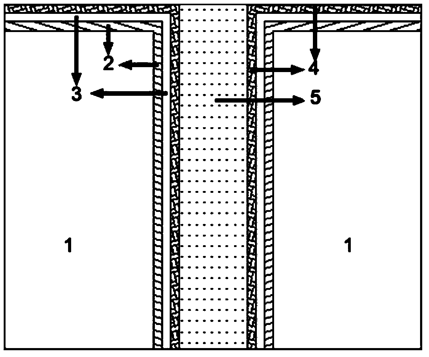
[0047] (2) Preparation of the transmission electron microscope sample at the upper part of the TSV (the distance from the upper surface of the through hole is 5 μm), and the large through-hole structure substrate is cut into 4×4mm with a glass knife 2 Put the small pieces into the adhesive diluted with acetone and soak for 5 minutes.

[0048] (3) Vibrate the sample placed in the adhesive diluted with acetone with an ultrasonic cleaner; wherein, the adhesive is 502 adhesive with α-ethyl cyanoacrylate as the main component, and the volume ratio of the adhesive to acetone is 10 ﹪; take out the ultrasonically sounded sample and place it in the air, after the acetone is completely evaporated, the liquid adhesive solidifies in the TSV.

[0049] (4) The surface of the sample is stuck on a glass sheet of a certain thickness, and the sample is ground to the th...

Embodiment 3

[0052] (1) The TSV through hole is a blind hole, and the size of the through hole is: 50 μm in diameter and 100 μm in depth.

[0053] (2) The preparation of the transmission electron microscope sample at the middle position of the TSV (the distance from the upper surface of the through hole is 50 μm) will be cut into 5×5mm with a glass knife 2 Small pieces of samples with TSVs were placed in an adhesive diluted with acetone and soaked for 10 minutes.

[0054] (3) Use an ultrasonic cleaner to oscillate the sample placed in the acetone-diluted adhesive (oscillate for 5 minutes); wherein, the adhesive is 502 adhesive mainly composed of α-ethyl cyanoacrylate, and the volume ratio of adhesive to acetone is 1: 5. Take out the ultrasonically sounded sample and place it in the air, so that the liquid adhesive solidifies in the TSV after the acetone is completely evaporated.

[0055] (4) Stick the lower surface of the sample on a glass sheet of a certain thickness, grind the sample to...


PUM

PropertyMeasurementUnit
diameteraaaaaaaaaa

Abstract

The invention discloses a method for preparing a micro intercommunicated hole structure transmission electron microscope sample. The method includes the steps that a hollow through hole is filled with adhesive diluted with acetone, the solidified adhesive covers the inner wall of the through hole, tissue of interface layers such as an insulation layer, a barrier layer and a copper seed layer on a through hole base body are protected and foreign matter is prevented from entering the through hole; then, according to the position of the through hole needing to be observed, after samples are ground from the upper surfaces and the lower surfaces to be within the range of hole depths needing to be inspected through thickness measurement, according to a conventional ion thinning method, the through hole region is aligned, thinned and perforated, a plane transmission electron microscope sample of the inner wall of the through hole is obtained, and then the tissue of the interface layers at different hole depths of the through hole samples is accurately positioned and represented. According to the method, ionic contamination cannot be introduced into the samples, a sample preparation device is simple, low in cost and convenient to operate, and a feasible plane sample preparation method is provided for through hole type micro-electronic interconnected structure and semiconductor device transmission electron microscope tissue observation.

Description

technical field [0001] The invention relates to the technical field of microelectronic three-dimensional packaging through-hole interconnection technology and semiconductor device manufacturing technology, in particular to a method for preparing a micro-interconnection through-hole structure transmission electron microscope sample, which can realize all interfaces at any position required by the through-hole structure sample Precise positioning characterization of layers. Background technique [0002] Moore's Law "The integration level of integrated circuits (IC) doubles every 18 months, and the performance will also double". development in the direction of miniaturization. However, the traditional two-dimensional planar miniaturization strategy has reached the limit of performance, silicon process size and manufacturing cost, and is gradually being adopted by a new generation of three-dimensional (3D) semiconductor integrated packaging technology, such as stacked, through-...

Claims


Application Information

Patent Timeline
Patent Type & Authority Applications(China)
IPC IPC(8): G01N1/28
Inventor 刘志权田飞飞李财富曹丽华
Owner INST OF METAL RESEARCH - CHINESE ACAD OF SCI
Why Eureka
Try Eureka