Formation method of interfacial layer and formation method of metal gate transistor
A metal gate and interface layer technology, applied in the manufacture of transistors, semiconductor devices, semiconductor/solid-state devices, etc., can solve problems such as poor stability and interface defects between high-K dielectric layers and silicon substrates
- Summary
- Abstract
- Description
- Claims
- Application Information
AI Technical Summary
Problems solved by technology
Method used
Image

Examples
Embodiment 1
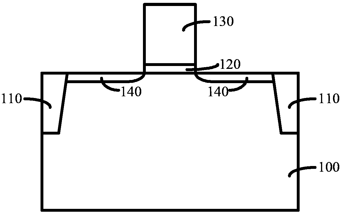
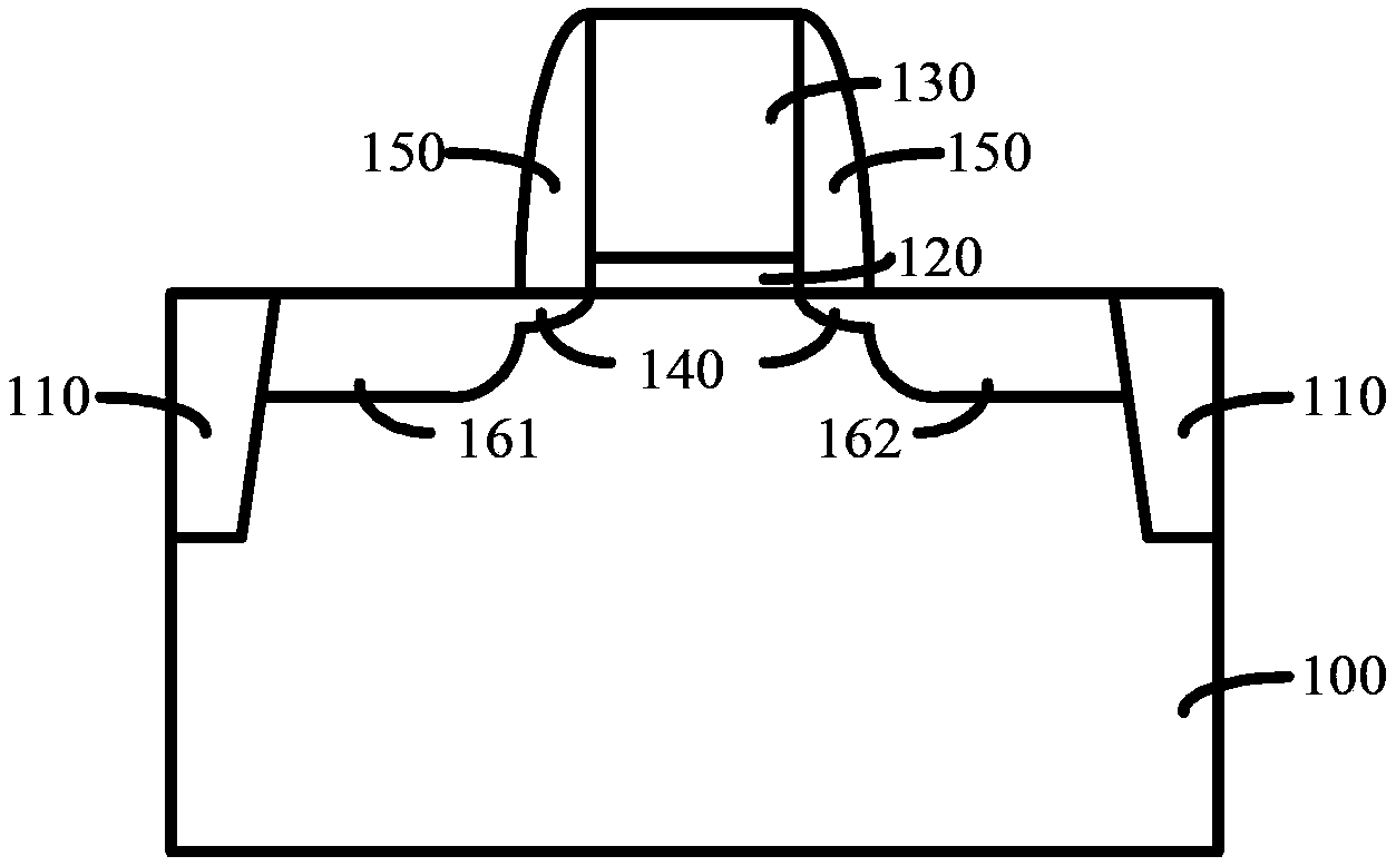
[0062] Such as figure 1 As shown, step S1 is first performed: providing a semiconductor substrate 100 .
[0063] The semiconductor substrate 100 is a commonly used substrate material such as a bulk silicon (bulk silicon) substrate or a silicon-on-insulator (SOI) substrate, and can also be doped into the semiconductor substrate 100 such as germanium, indium arsenide, lead telluride, materials such as gallium telluride. A shallow trench isolation structure 110 is formed in the semiconductor substrate 100 to isolate the metal gate transistor from other devices formed on the semiconductor substrate 100 .
[0064] Continue to refer to figure 1 As shown, step S2 is then performed: forming a dummy gate 130 on the semiconductor substrate 100 .
[0065] In one embodiment, the method for forming the dummy gate 130 includes: forming an etch stop layer on the semiconductor substrate 100; forming a dummy gate material layer on the etch stop layer, the material of which can be polysili...
Embodiment 2
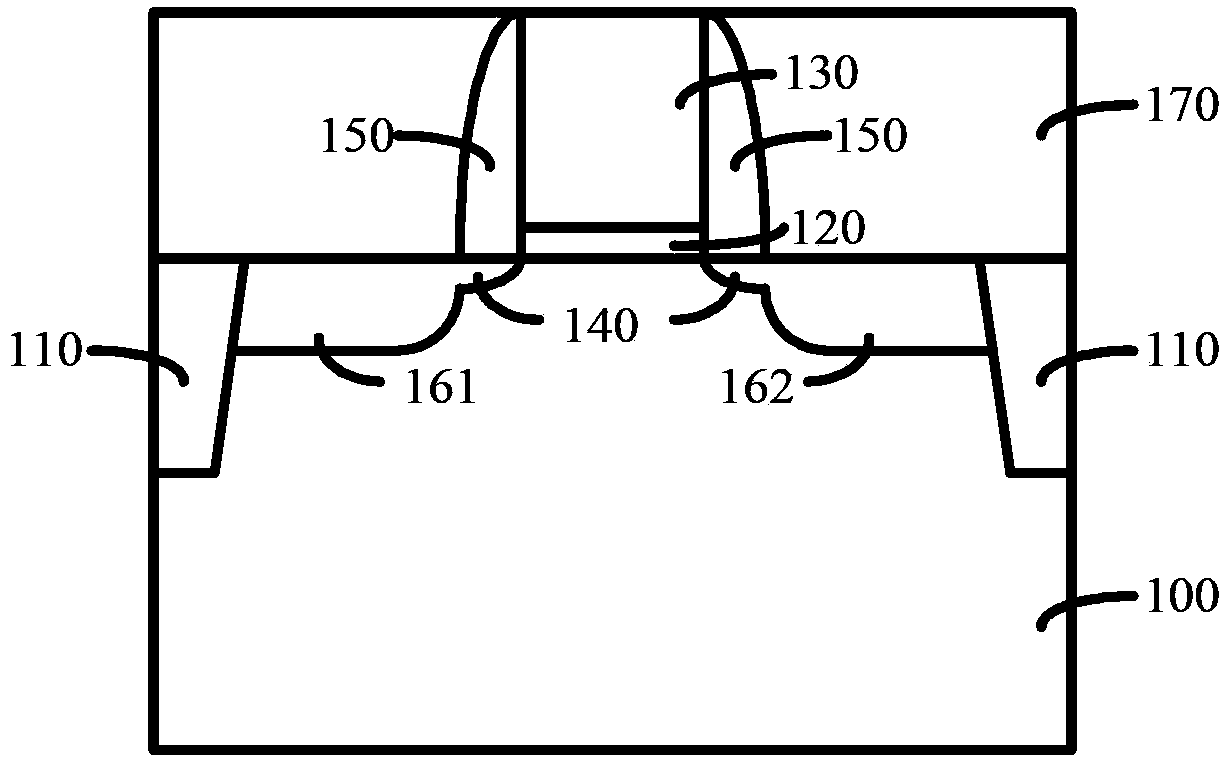
[0087] Such as Figure 8 As shown, step S11 is first performed: providing a semiconductor substrate 200 .
[0088] A shallow trench isolation structure 210 is formed in the semiconductor substrate 200 to isolate the metal gate transistor from other devices formed in the semiconductor substrate 200 . For more specific content of this step, reference may be made to step S1 in Embodiment 1, which will not be repeated in this embodiment.
[0089] Continue to refer to Figure 8 As shown, step S12 is then performed: forming a high-K dielectric layer 220 on the semiconductor substrate 100 .
[0090] The specific material and formation method of the high-K dielectric layer 220 can refer to Embodiment 1, and will not be repeated here.
[0091] Continue to refer to Figure 8 As shown, step S13 is then performed: forming an interface layer 230 on the surface of the semiconductor substrate 100 in contact with the high-K dielectric layer 220 .
[0092] The method for forming the inter...
PUM
 Abstract
Description
Claims
Application Information
 - R&D
- Intellectual Property
- Life Sciences
- Materials
- Tech Scout
- Unparalleled Data Quality
- Higher Quality Content
- 60% Fewer Hallucinations
Browse by: Latest US Patents, China's latest patents, Technical Efficacy Thesaurus, Application Domain, Technology Topic, Popular Technical Reports.
© 2025 PatSnap. All rights reserved.Legal|Privacy policy|Modern Slavery Act Transparency Statement|Sitemap|About US| Contact US: help@patsnap.com