Unlock instant, AI-driven research and patent intelligence for your innovation.

Method for forming semiconductor structure

A technology of semiconductor and stack structure, which is applied in semiconductor devices, semiconductor/solid-state device manufacturing, electric solid-state devices, etc., to achieve the effect of simple and convenient process.

Active Publication Date: 2014-10-29
SEMICON MFG INT (SHANGHAI) CORP
View PDF8 Cites 16 Cited by
  • Summary
  • Abstract
  • Description
  • Claims
  • Application Information

AI Technical Summary

Problems solved by technology

[0007] Due to the huge difference between the structure of the fin field effect transistor and the structure of the flash memory, the compatible manufacturing process of the fin field effect transistor and the flash memory faces great challenges

Method used


Image

  • Method for forming semiconductor structure
  • Method for forming semiconductor structure
  • Method for forming semiconductor structure

Examples


Embodiment Construction

[0035] As mentioned in the background, the existing methods for forming FinFETs are not compatible with the methods for manufacturing flash memories.

[0036] The embodiment of the present invention provides a method for forming a semiconductor structure. The fin field effect transistor is formed at the same time as the flash memory unit, and the process is simple and convenient.

[0037] In order to make the above objects, features and advantages of the present invention more comprehensible, specific implementations of the present invention will be described in detail below in conjunction with the accompanying drawings.

[0038] Figure 3 ~ Figure 17 It is a structural schematic diagram of a method for forming a semiconductor structure according to an embodiment of the present invention.

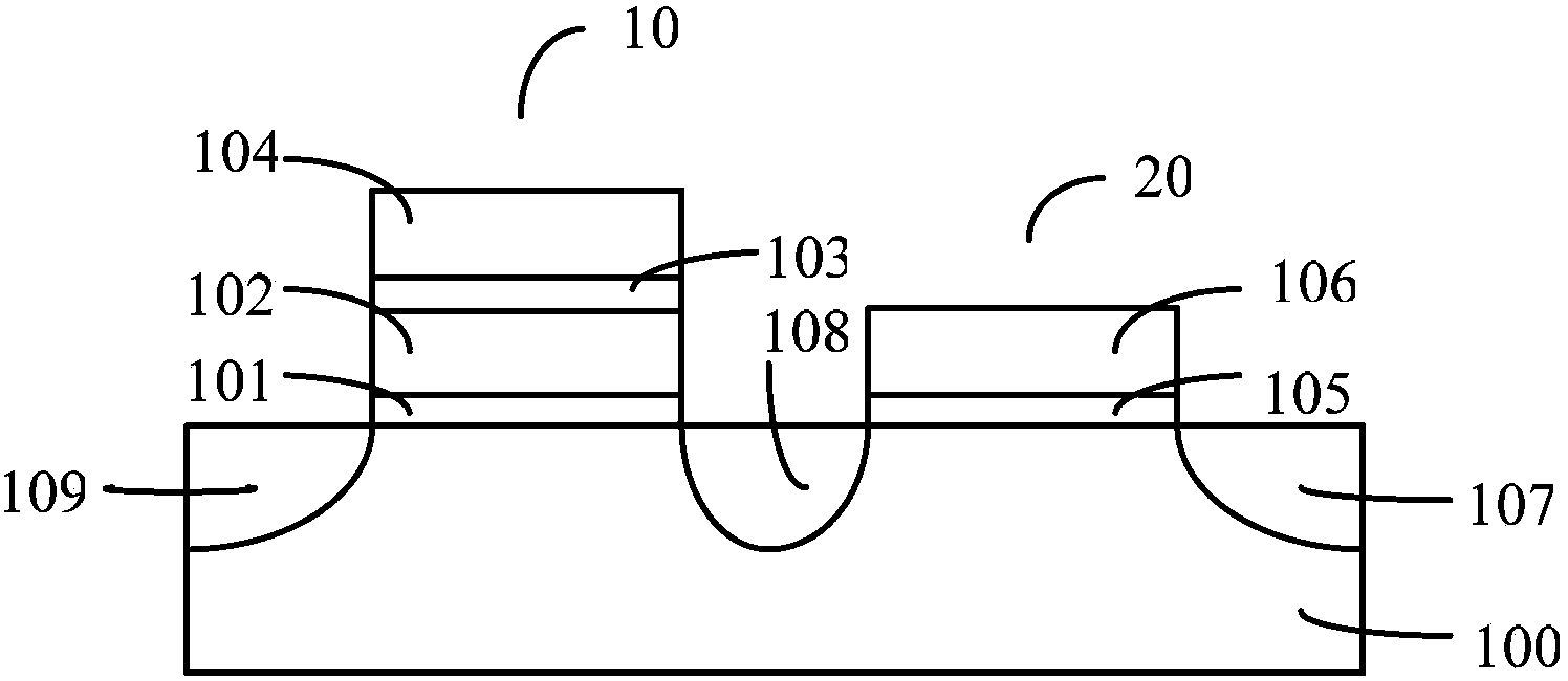
[0039] First, refer to image 3 , provide a semiconductor substrate 300, the semiconductor substrate 300 includes a peripheral region 31 and a storage region 32, the peripheral region 31 ...


PUM

PropertyMeasurementUnit
Thicknessaaaaaaaaaa
Thicknessaaaaaaaaaa
Thicknessaaaaaaaaaa

Abstract

A method for forming a semiconductor structure comprises the steps of providing a semiconductor substrate, forming a plurality of split stacking structures on the semiconductor substrate, enabling first silicon oxide layers in the stacking structures of a storage region to serve as tunneling oxidation layers of a flash memory unit, and enabling a first polycrystalline silicon layer to serve as a floating gate of the flash memory unit; utilizing the stacking structures as masks to etch the semiconductor substrate, forming first grooves in a peripheral region and the storage region of the semiconductor substrate, enabling the semiconductor substrate between the adjacent first grooves in the peripheral region to form a first fin; forming an isolation layer on the semiconductor substrate and performing etching to remove part of the isolation layer of the peripheral region; removing the stacking structures on the peripheral region and exposing the top surface of the first fin; forming a first gate structure of a fin type field-effect transistor on a side wall and the top surface of the first fin of the peripheral region, and forming a control gate of the flash memory unit on the floating gate of the storage region. A process for forming the flash memory unit is compatible with a process for manufacturing the fin type field-effect transistor.

Description

technical field [0001] The invention relates to the field of semiconductor manufacturing, in particular to a method for forming a semiconductor structure. Background technique [0002] In the current semiconductor industry, integrated circuit products can be mainly divided into three types: analog circuits, digital circuits and digital / analog hybrid circuits, among which storage devices are an important type of digital circuits. In recent years, among storage devices, a flash memory (flash memory, referred to as a flash memory unit) has developed particularly rapidly. The main feature of the flash memory unit is that it can keep the stored information for a long time without power on; and it has the advantages of high integration, fast access speed, easy erasing and rewriting, etc. Has been widely used. [0003] As an important flash memory, an erasable programmable read-only memory (Electrically Erasable Programmable ROM, EEPROM) has been widely used. figure 1 It is a sc...

Claims


Application Information

Patent Timeline
IPC IPC(8): H01L21/8247H01L21/336
CPCH01L29/66795H10B41/00
Inventor 三重野文健
Owner SEMICON MFG INT (SHANGHAI) CORP
Features
  • R&D
  • Intellectual Property
  • Life Sciences
  • Materials
  • Tech Scout
  • Unparalleled Data Quality
  • Higher Quality Content
  • 60% Fewer Hallucinations
Learn More