Supercharge Your Innovation With Domain-Expert AI Agents!

A si/nio:na heterogeneous pn junction diode

A pn junction and diode technology, applied in the field of Si/NiO:Na heterogeneous pn junction diodes, to achieve the effect of improving performance

Inactive Publication Date: 2018-04-10
TIANJIN UNIV OF TECH & EDUCATION TEACHER DEV CENT OF CHINA VOCATIONAL TRAINING & GUIDANCE
View PDF5 Cites 0 Cited by
  • Summary
  • Abstract
  • Description
  • Claims
  • Application Information

AI Technical Summary

Problems solved by technology

This choice is of great significance for the development of new devices, but there is no report for Si / NiO:Na heterojunction

Method used


Image

  • A si/nio:na heterogeneous pn junction diode
  • A si/nio:na heterogeneous pn junction diode
  • A si/nio:na heterogeneous pn junction diode

Examples


preparation example Construction

[0019] (2) Preparation of p-NiO:Na: the background vacuum of the chamber before sputtering is better than 3x10 -4 Pa, the relative partial pressure of oxygen used O 2 / (O 2 +Ar)=0%-100%, the sputtering pressure is 0.5-2Pa, and the sputtering power is 100-200W. Before coating, pre-sputter for 5 min to remove impurities on the target surface. The coating time is 20-120 minutes, the substrate temperature is RT-600° C. and the temperature is 200° C. to 700° C. and annealed for 0.5 to 1 hour.

[0020] (3) Electrode preparation: use methods such as sputtering or thermal evaporation (such as: Tang Weizhong, the principle, technology and application of thin film material preparation, Metallurgical Industry Press, 1998 first edition) to make nickel / aluminum on the surface of NiO:Na and Si / gold electrode.

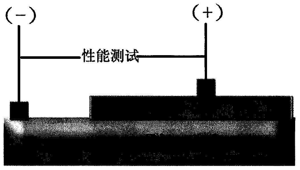
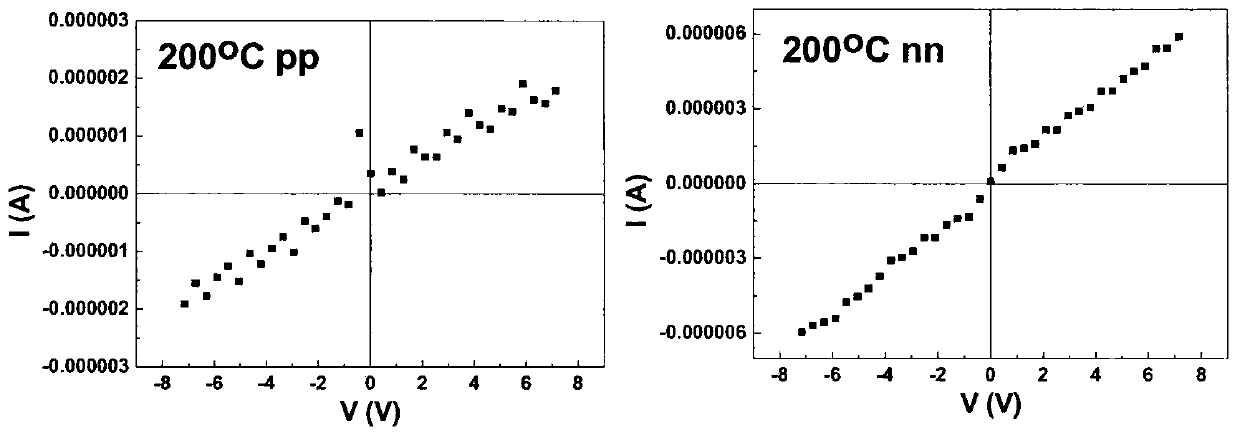
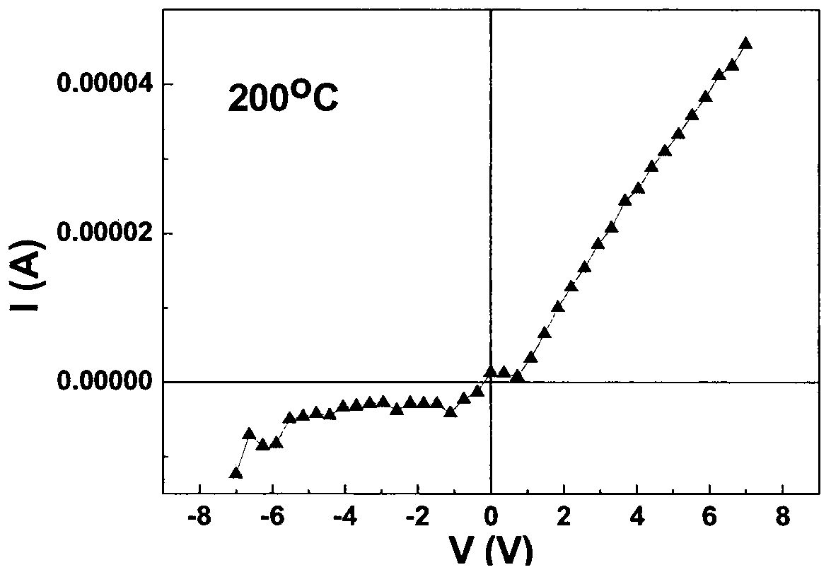
[0021] (4) Test the ohmic contact characteristics of the detection electrode with Keithley2612A and the I-V characteristics (rectification characteristics) of the heterogeneous...

Embodiment 1

[0023] (1) Clean the silicon wafer with the cleaning method in the semiconductor process and dry it with nitrogen;

[0024] (2) Preparation of p-NiO:Na: A NiO:Na ceramic target with a diameter of 50 mm was used. NiO:Na films prepared by magnetron sputtering. The chamber background vacuum before sputtering is better than 3x10 -4 Pa, the relative partial pressure of oxygen used O 2 / (O 2 +Ar) = 100%. The sputtering pressure is 2Pa, and the sputtering power is 200W. Before coating, pre-sputter for 5 min to remove impurities on the target surface. The coating time is 120min, the substrate temperature is RT, and annealed at 200°C for 0.5 hours in the later stage.

[0025] (3) Electrode preparation: Ni electrodes were fabricated on the edges of NiO:Na and Si surfaces by thermal evaporation.

[0026] (4) Test the ohmic contact characteristics of Keithley2612A detection electrodes and the I-V characteristics (rectification characteristics) of heterogeneous pn junction diodes, s...

Embodiment 2

[0028] (1) Clean the silicon wafer with the cleaning method in the semiconductor process and dry it with nitrogen;

[0029] (2) Preparation of p-NiO:Na: A NiO:Na ceramic target with a diameter of 50 mm was used. NiO:Na films prepared by magnetron sputtering. The chamber background vacuum before sputtering is better than 3x10 -4 Pa, the relative partial pressure of oxygen used O 2 / (O 2 +Ar) = 100%. The sputtering pressure is 2Pa, and the sputtering power is 200W. Before coating, pre-sputter for 5 min to remove impurities on the target surface. The coating time is 120min, the substrate temperature is RT, and annealed at 300°C for 0.5 hours in the later stage.

[0030] (3) Electrode preparation: Ni electrodes were fabricated on the edges of NiO:Na and Si surfaces by thermal evaporation.

[0031] (4) Test the ohmic contact characteristics of Keithley2612A detection electrodes and the I-V characteristics (rectification characteristics) of heterogeneous pn junction diodes, s...


PUM

PropertyMeasurementUnit
transmittivityaaaaaaaaaa
diameteraaaaaaaaaa

Abstract

The invention discloses an Si / NiO:Na hetero-pn-junction diode comprising at least a pn-junction and an ohmic contact electrode. The pn-junction is a hetero-pn-junction formed by growing a p-type NiO:Na film on an Si substrate. According to the invention, the magnetron sputtering process is used for preparing the p-type NiO:Na film on the Si substrate, and finally, the magnetron sputtering or thermal evaporation method is used for producing an electrode on the pn-junction. The hetero-pn-junction diode in the invention has high reverse breakdown voltage and large forward current density, and is simple in preparation process and low in cost.

Description

Technical field [0001] The invention relates to a Si / NiO:Na heterogeneous pn junction diode. The invention belongs to the field of functional materials and optoelectronic devices. Background technique [0002] The internal degrees of freedom of the d(f) electrons contained in the strongly correlated material NiO, such as the interaction between spin, charge, and orbit, make NiO exhibit many exotic properties, and at the same time make the physical properties of the material vary with internal parameters such as temperature , pressure, and doping changes significantly. So far, NiO has been used in the research of catalysts, battery electrodes, electrochemical capacitors and other fields because of its good catalytic performance and thermal sensitivity, but there are few reports on its photoelectric properties. Semiconductor heterojunctions are easy to realize the separation of photogenerated charges and are widely used in the research and development of optoelectronic devic...

Claims


Application Information

Patent Timeline
Patent Type & Authority Patents(China)
IPC IPC(8): H01L29/861H01L29/12H01L21/329
CPCH01L21/02631H01L29/0688H01L29/24H01L29/66969H01L29/861
Inventor 李彤
Owner TIANJIN UNIV OF TECH & EDUCATION TEACHER DEV CENT OF CHINA VOCATIONAL TRAINING & GUIDANCE
Features
  • R&D
  • Intellectual Property
  • Life Sciences
  • Materials
  • Tech Scout
  • Unparalleled Data Quality
  • Higher Quality Content
  • 60% Fewer Hallucinations
Learn More