Method for manufacturing GaN epitaxial wafers or GaN substrates

A manufacturing method and substrate technology, which are applied in semiconductor/solid-state device manufacturing, electrical components, circuits, etc., can solve the problems of large stress, lattice mismatch, and thermal expansion coefficient difference between GaN and Si, and reduce the contact area, reduce Production cost, stress reduction effect

Inactive Publication Date: 2014-11-12
SHANGHAI HUAHONG GRACE SEMICON MFG CORP
View PDF6 Cites 9 Cited by
  • Summary
  • Abstract
  • Description
  • Claims
  • Application Information

AI Technical Summary

Problems solved by technology

However, it is difficult to grow GaN single crystals at present, and it is difficult to obtain high-quality, large-size, and low-cost GaN single crystals.
There are two main reasons why GaN is difficult to grow on Si substrates: one is the lattice mismatch, and the mismatch degree between the two i

Method used


Image

  • Method for manufacturing GaN epitaxial wafers or GaN substrates
  • Method for manufacturing GaN epitaxial wafers or GaN substrates
  • Method for manufacturing GaN epitaxial wafers or GaN substrates

Examples


Embodiment Construction

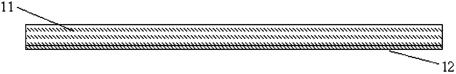
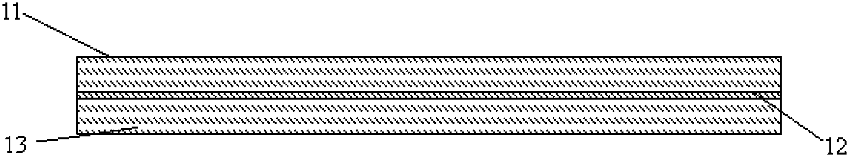
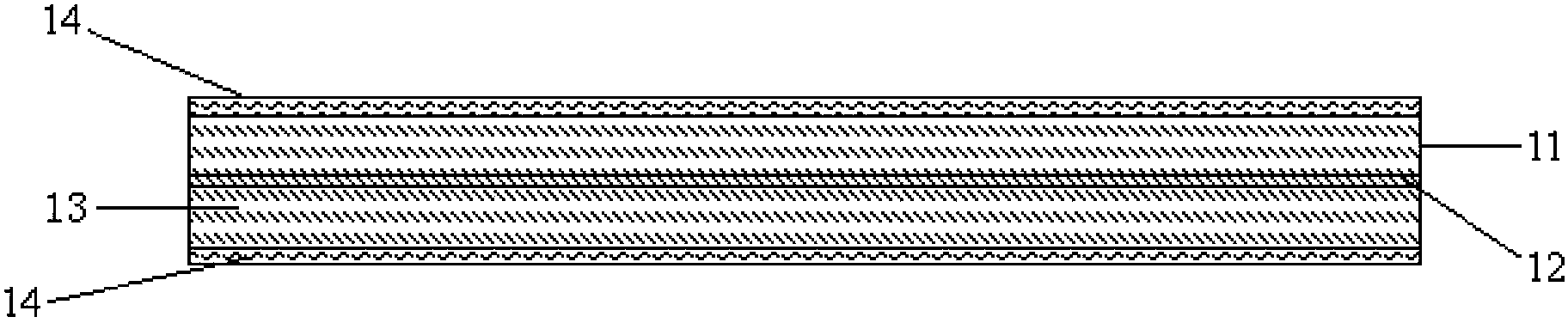
[0028] The fabrication method of GaN epitaxy or GaN substrate of the present invention, comprises the following steps:

[0029] 1) Using a thermal oxidation process or chemical vapor deposition (CVD), grow silicon oxide 12 on the back of the first silicon substrate 11 with a thickness of 0.01-2.0 μm (such as figure 1 shown);

[0030] 2) The back side of the first silicon substrate 11 with silicon oxide 12 and the back side of the second silicon substrate 13 are bonded together through Si-O at 1250-1400°C to form a third silicon substrate (such as figure 2 shown);

[0031] 3) Using chemical vapor deposition (CVD), growing silicon nitride or silicon oxynitride 14 on the upper and lower surfaces of the third silicon substrate, wherein the thickness of silicon nitride or silicon oxynitride on each surface is 0.1-5.0 μm ( like image 3 shown);

[0032] 4) Using the method of anisotropic dry etching, silicon nitride or silicon oxynitride 14 on the third silicon substrate is etc...


PUM

PropertyMeasurementUnit
Thicknessaaaaaaaaaa
Thicknessaaaaaaaaaa
Thicknessaaaaaaaaaa

Abstract

The invention discloses a method for manufacturing GaN epitaxial wafers or GaN substrates. The method comprises the steps that (1) silicon oxide is grown on the back surface of a first silicon substrate; (2) the back surface of the first silicon substrate with the silicon oxide is bonded to the back surface of a second silicon substrate so that a third silicon substrate can be formed; (3) silicon nitride or silicon oxynitride are grown on the upper surface and the lower surface of the third silicon substrate; (4) the silicon nitride or silicon oxynitride on the third silicon substrate is etched in a double-surface mode so as to form required patterns; (5) GaN selective epitaxial growth is conducted on the double surfaces of the third silicon substrate; (6) the first silicon substrate and the second silicon substrate are stripped, so that the two GaN epitaxial wafers or the two GaN substrates are formed. According to the method for manufacturing the GaN epitaxial wafers or the GaN substrates, the GaN stress can be relieved effectively, GaN crazing and lattice defects can be overcome, and meanwhile the growth cost can be reduced.

Description

technical field [0001] The present invention relates to a method for manufacturing epitaxy or substrate in semiconductor integrated circuits, in particular to a method for making GaN (gallium nitride) epitaxy or GaN substrate. Background technique [0002] GaN is a wide bandgap semiconductor material, which has excellent physical and chemical properties, such as large bandgap width, high breakdown electric field strength, high saturation electron drift velocity, high thermal conductivity and strong radiation resistance, thermal conductivity and Large dielectric constant, stable chemical properties, etc., especially suitable for making semiconductor devices used in high-voltage, high-temperature, high-frequency, high-power, and strong-irradiation environments. Specifically, the band gap of GaN is larger than that of Si material, and the intrinsic carrier concentration is lower than that of Si, which determines that the limit operating temperature of GaN-based devices is highe...

Claims


Application Information

Patent Timeline
IPC IPC(8): H01L21/02H01L21/205
CPCH01L21/6835H01L21/02381H01L21/02488H01L21/02499H01L21/02502H01L21/02513H01L21/0254
Inventor 刘继全彭仕敏
Owner SHANGHAI HUAHONG GRACE SEMICON MFG CORP
Why Eureka
Try Eureka