Chemical-mechanical polishing pad

A chemical machinery and polishing pad technology, applied in the direction of grinding tools, etc., can solve the problems that the polishing liquid cannot be distributed quickly and reasonably, affect the polishing speed and removal rate, and reduce the use effect of the polishing pad, so as to improve the polishing speed and polishing effect, and speed up the polishing process. Chemical corrosion speed, good polishing effect

Inactive Publication Date: 2014-11-19
HUBEI DINGLONG CO LTD
View PDF5 Cites 13 Cited by
  • Summary
  • Abstract
  • Description
  • Claims
  • Application Information

AI Technical Summary

Problems solved by technology

The above two structures can play a role in storing the polishing liquid to a certain extent when they are used in the initial stage, but after a period of operation, the following problems will occur: (1) The slag discharge is not smooth, and the polishing debris and silicon wafers cannot be removed. After the smooth discharge of debris, the particles in the polishing liquid will block the grooves or holes on the polishing layer, resulting in a decline in the use of the polishing pad; (2) due to poor slag discharge, the blocked grooves and holes will also bring Scratches will further affect the polishing speed and removal rate, and even affect the polishing effect
(3) The polishing liquid cannot be distributed quickly and reasonably on the polishing pad, thus further affecting the polishing speed

Method used


Image

  • Chemical-mechanical polishing pad
  • Chemical-mechanical polishing pad
  • Chemical-mechanical polishing pad

Examples


Embodiment

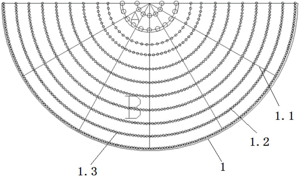
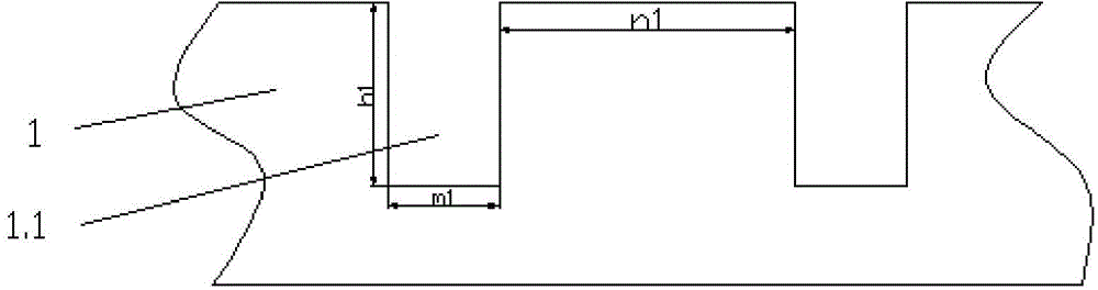
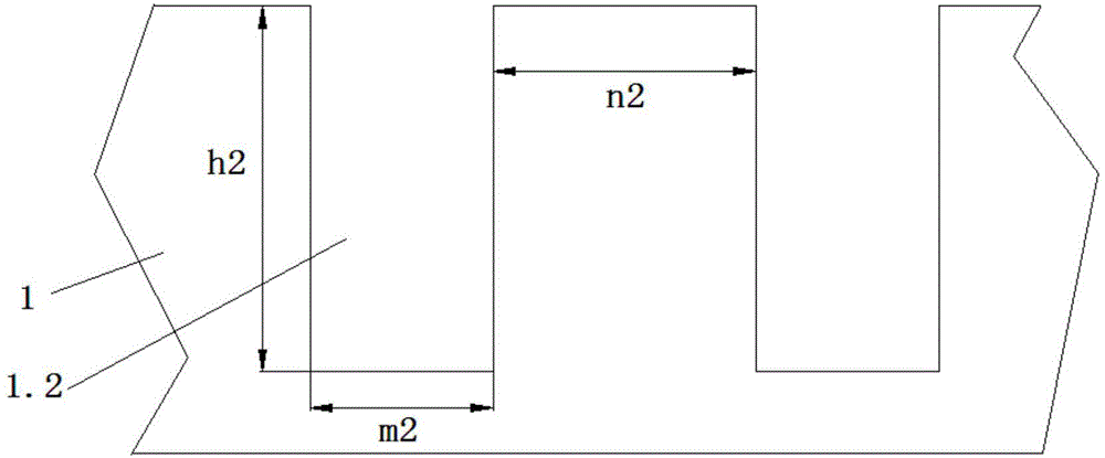
[0042] According to the conventional pouring method of polyurethane, water-insoluble hollow microspheres (such as EXPANCEL551DE40d42 manufactured by Akzo Nobel, with a diameter distribution of 10 μm-100 μm) are added to the polyurethane polymer and mixed, and the mixture is poured into the mold and matured at high temperature to obtain a diameter of 680mm , a rectangular plate with a thickness of 2.5mm. Then use a cutting machine (such as Beijing Jingdiao Technology Group Co., Ltd.) to cut into a disc-shaped polishing layer with a diameter of 650mm. Take the center of the polishing surface of polishing layer 1 as the endpoint, and uniformly process n1 lines extending to the edge of the polishing surface. The groove 1.1 is used to divide the polished surface into n1 equal parts. The width m1 of the groove 1.1, the depth h1 (see figure 2 ). With the center of the polished surface as the center of the circle, the plurality of holes 1.2 are arranged into multiple rows of concen...

experiment example

[0047] Standard polishing pads (such as IC1000 and IC1010 of DOW Company of the United States) commonly used in the market for chip polishing were compared with the polishing pad of the present invention for polishing performance evaluation.

[0048] The polishing pads in Examples 1-20 and Comparative Examples are respectively installed on the fixed plate of the polishing device (manufactured by Suzhou Heruite Electronic Special Equipment Technology Co., Ltd., "9B type", "16B type" polishing machine), fixed plate The rotation speed is at 40rpm, and the wafer is polished for 10 minutes with a twice-diluted chemical polishing solution (Jiangsu Zhongjing Optoelectronics Co., Ltd., g-CUT5003SC type) at a flow rate of 300cc / min. The state of polishing speed, scratches, foreign matter and voids.

[0049] Each measurement method is as follows:

[0050] (1) Polishing speed: The film thickness of the wafer before and after polishing was measured with an optical film thickness measurin...


PUM


Abstract

The invention discloses a chemical-mechanical polishing pad and solves the problem that an existing polishing pad is scratched easily and low in polishing efficiency. According to the technical scheme, the chemical-mechanical polishing pad comprises a polishing layer, a plurality of holes are formed in the polishing surface of the polishing layer, the center of the polishing surface is a circle center, and the holes are arranged into multiple rows of concentric rings different in diameter. The center of the polishing surface is an end point, and a plurality of grooves extending to the edge of the polishing surface are evenly radiated from the end point. The surface roughness of the polishing surface is below 15 micrometers. The polishing pad is simple in structure, capable of increased polishing removing efficiency and inhibiting scratches, and long in service life.

Description

technical field [0001] The invention relates to a polishing pad for chemical mechanical planarization treatment, in particular to a chemical mechanical polishing pad. Background technique [0002] Chemical mechanical planarization, or chemical mechanical polishing (CMP), is a common technique used to planarize semiconductor wafers, substrates such as sapphire. In conventional CMP, a wafer is mounted on a holder assembly and brought into contact with a polishing pad on a polishing plate in a CMP apparatus. The support assembly provides controlled pressure on the wafer, pressing the wafer against the polishing pad. The external driving force makes the polishing pad rotate relative to the wafer. At the same time, a chemical composition or other polishing solution is provided between the wafer and the polishing pad. Thus, the surface of the wafer is polished and flattened by the chemical and mechanical action of the polishing pad surface and the slurry. [0003] In the CMP s...

Claims


Application Information

Patent Timeline
Patent Type & Authority Applications(China)
IPC IPC(8): B24B37/24B24B37/26
CPCB24B37/24B24B37/26
Inventor 朱顺全梅黎黎李云峰
Owner HUBEI DINGLONG CO LTD
Why Eureka
Try Eureka