
Treatment method for unqualified silicon wafers

A processing method and technology for silicon wafers, applied in photovoltaic power generation, electrical components, climate sustainability, etc., can solve problems such as instability, complex manufacturing process, affecting product production qualification rate, etc., to avoid waste of resources and improve production. The effect of pass rate

Active Publication Date: 2014-11-19
HAINAN YINGLI NEW ENERGY
View PDF4 Cites 5 Cited by
  • Summary
  • Abstract
  • Description
  • Claims
  • Application Information

AI Technical Summary

Problems solved by technology

Among them, due to the complex manufacturing process, before the screen printing process, that is, in the texturing-coating process, due to equipment instability or human misoperation, a large number of unqualified silicon wafers often appear in the production process. Unqualified silicon wafers directly affect the production qualification rate of products

Method used


Image

  • Treatment method for unqualified silicon wafers

Examples


Embodiment Construction

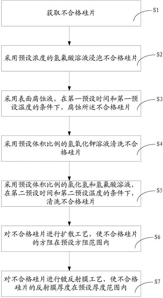
[0032] The following will clearly and completely describe the technical solutions in the embodiments of the present invention with reference to the accompanying drawings in the embodiments of the present invention. Obviously, the described embodiments are only some, not all, embodiments of the present invention. Based on the embodiments of the present invention, all other embodiments obtained by persons of ordinary skill in the art without making creative efforts belong to the protection scope of the present invention.

[0033] As mentioned in the background technology, due to the complicated process of making solar cells, before the screen printing process, that is, in the texturing-coating process, due to equipment instability or human misoperation, etc., a large number of solar cells often appear in the production process. Unqualified silicon wafers, these unqualified silicon wafers directly affect the production qualification rate of products.

[0034] Based on this, the e...


PUM

PropertyMeasurementUnit
Thicknessaaaaaaaaaa
Thicknessaaaaaaaaaa

Abstract

The invention discloses a treatment method for unqualified silicon wafers. The treatment method comprises the steps that the unqualified silicon wafers are obtained; a hydrofluoric acid solution with a preset concentration is used for soaking the unqualified silicon wafers; a surface corrosive liquid is adopted for corroding the unqualified silicon wafers under the conditions of a first preset time and a first preset temperature; a potassium hydroxide solution with a preset volume fraction is adopted for cleaning the unqualified silicon wafers; a hydrogen chloride and hydrofluoric acid solution with a preset volume fraction is adopted for cleaning the unqualified silicon wafers under the conditions of a second preset time and a second preset temperature; a diffusion technology is carried out on the unqualified silicon wafers so that sheet resistance of the unqualified silicon wafers can be within a preset range of sheet resistance; a reflectance coating plating technology is carried out on the unqualified silicon wafers so that the thickness of reflectance coatings of the unqualified silicon wafers can be within a preset thickness range. By the adoption of the technical scheme, after the unqualified silicon wafers produced before a silk-screen printing technology is performed are treated, the unqualified silicon wafers can be recycled for manufacturing solar cells, resource waste is avoided, and the production yield of products is increased.

Description

technical field [0001] The invention relates to the technical field of solar cells, and more specifically, relates to a processing method for unqualified silicon chips. Background technique [0002] The environmental pollution caused by traditional fossil energy power generation is threatening the environment on which human beings live. Therefore, it is imperative to develop a green and pollution-free energy source. Solar cells, also known as photovoltaic cells, are semiconductor devices that directly convert the sun's light energy into electrical energy. Because they are green and environmentally friendly products, they will not cause environmental pollution. Therefore, in today's energy shortage situation, solar cells are A new type of product with development prospects. [0003] Generally, the manufacturing process of crystalline silicon solar cells includes: texturing-PN junction diffusion-etching-coating-screen printing-sintering. Among them, due to the complex manufa...

Claims


Application Information

Patent Timeline
IPC IPC(8): H01L31/18H01L21/02
CPCH01L21/02032H01L31/1804Y02E10/547Y02P70/50
Inventor 许明金符昌京邓清龙陈耀军
Owner HAINAN YINGLI NEW ENERGY
Features
  • Generate Ideas
  • Intellectual Property
  • Life Sciences
  • Materials
  • Tech Scout
  • Unparalleled Data Quality
  • Higher Quality Content
  • 60% Fewer Hallucinations
Learn More