GaN-based light-emitting diode structure improving light extraction rate and preparation method

A light-emitting diode, gallium nitride-based technology, applied in the direction of electrical components, circuits, semiconductor devices, etc., can solve the problems of low sub-concentration, low light extraction efficiency, uneven current distribution, etc., to overcome the complexity of the process and improve the current carrying capacity Sub concentration, the effect of improving the uniformity of current distribution

Active Publication Date: 2014-11-19
太原理工大学建筑设计研究院有限公司
View PDF10 Cites 12 Cited by
  • Summary
  • Abstract
  • Description
  • Claims
  • Application Information

AI Technical Summary

Problems solved by technology

[0004] In order to solve the technical problems of low carrier concentration in the P-type region of the current LED structure, uneven current distribution and lo...

Method used


Image

  • GaN-based light-emitting diode structure improving light extraction rate and preparation method
  • GaN-based light-emitting diode structure improving light extraction rate and preparation method
  • GaN-based light-emitting diode structure improving light extraction rate and preparation method

Examples


Embodiment Construction

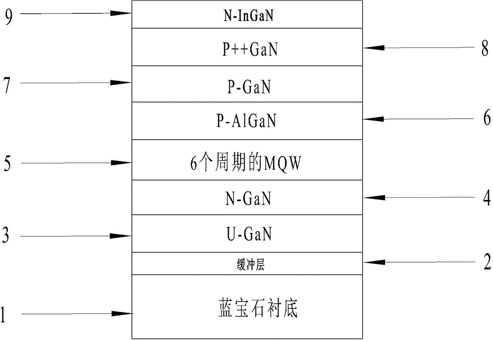
[0033] A gallium nitride-based light-emitting diode structure that improves the light extraction rate, the light-emitting diode structure includes: a substrate 1; a GaN buffer layer 2 grown on the substrate 1; a non-doped GaN buffer layer grown on the GaN buffer layer 2 a GaN layer 3; a Si-doped GaN layer 4 grown on the non-doped GaN layer 3; a 6-period multi-quantum well structure 5 grown on the Si-doped GaN layer 4, wherein the thickness of the well layer is 2.7nm, The thickness of the first five barrier layers is 13nm, and the thickness of the last barrier layer is 17nm; the p-AlGaN electron blocking layer 6 grown on the multi-quantum well structure 5; the Mg-doped p-type GaN layer grown on the p-AlGaN electron blocking layer 6 7; a heavily doped p-type GaN layer 8 grown on the Mg-doped p-type GaN layer 7; an n-type InGaN layer 9 grown on the heavily doped p-type GaN layer 8.

[0034] The substrate 1 is a sapphire substrate.

[0035] A method for preparing a gallium nitrid...


PUM

PropertyMeasurementUnit
Carrier concentrationaaaaaaaaaa
Thicknessaaaaaaaaaa
Thicknessaaaaaaaaaa

Abstract

The invention belongs to the field of photoelectric devices, and particularly relates to a GaN-based light-emitting diode structure improving the light extraction rate and a preparation method. The GaN-based light-emitting diode structure improving the light extraction rate and the preparation method solve the technical problems that the carrier concentration of a P-type area of an existing LED structure is not high, currents are distributed unevenly, and the light emitting efficiency is low. The GaN-based light-emitting diode structure improving the light extraction rate comprises a substrate, a GaN buffer layer growing on the substrate, a non-doped GaN layer growing on the GaN buffer layer, a Si-doped GaN layer growing on the non-doped GaN layer, multiple-quantum well structures, growing on the Si-doped GaN layer, of six periods, a p-AlGaN electronic blocking layer growing on the multiple-quantum well structures, a Mg-doped p-type GaN layer growing on the p-AlGaN electronic blocking layer, a heavily-doped p-type GaN layer growing on the Mg-doped p-type GaN layer, and an n-type InGaN layer growing on the heavily-doped p-type GaN layer. According to the GaN-based light-emitting diode structure improving the light extraction rate and the preparation method, the currents are distributed evenly, the light emitting efficiency is high, and the preparation process is simple.

Description

technical field [0001] The invention belongs to the field of photoelectric devices, and in particular relates to a gallium nitride-based light-emitting diode structure and a preparation method for improving the light extraction rate. Background technique [0002] LED (Light Emitting Diode, light emitting diode) is an electronic component that converts electrical energy into light energy. It has the characteristics of high brightness, low energy consumption, long life and fast response. It is a green and environmentally friendly solid light source. It has broad application prospects in lighting, display and other fields, especially now, with the reduction of the cost of LED With the improvement of efficiency and efficiency, the advantages of LEDs over other traditional light sources are gradually emerging, especially in the lighting field. The proportion is increasing, and the market prospect is getting better and better. Although the development and application of LED has b...

Claims


Application Information

Patent Timeline
IPC IPC(8): H01L33/06H01L33/32H01L33/00
CPCH01L33/007H01L33/06H01L33/14H01L33/22H01L33/32
Inventor 许并社尚林翟光美贾伟马淑芳梁建李天保梅伏洪贾志刚
Owner 太原理工大学建筑设计研究院有限公司
Why Eureka
Try Eureka