Epitaxial wafer of light emitting diode and manufacturing method thereof

A technology of light-emitting diodes and epitaxial wafers, which is applied in the direction of electrical components, circuits, semiconductor devices, etc., can solve the problem that the light efficiency of high-power chips is not large, and achieve the reduction of electron spillage, obvious effects, and improvement of photoelectric performance. Effect

Active Publication Date: 2014-11-19
HC SEMITEK SUZHOU
View PDF6 Cites 8 Cited by
  • Summary
  • Abstract
  • Description
  • Claims
  • Application Information

AI Technical Summary

Problems solved by technology

[0006] In order to solve the problem that there is not much room for improving the light efficiency of high-power chips in the prior art, an embodiment of the present invention provides a light-emitting diode epitaxial wafer and a manufacturing method thereof

Method used


Image

  • Epitaxial wafer of light emitting diode and manufacturing method thereof
  • Epitaxial wafer of light emitting diode and manufacturing method thereof
  • Epitaxial wafer of light emitting diode and manufacturing method thereof

Examples


Embodiment 1

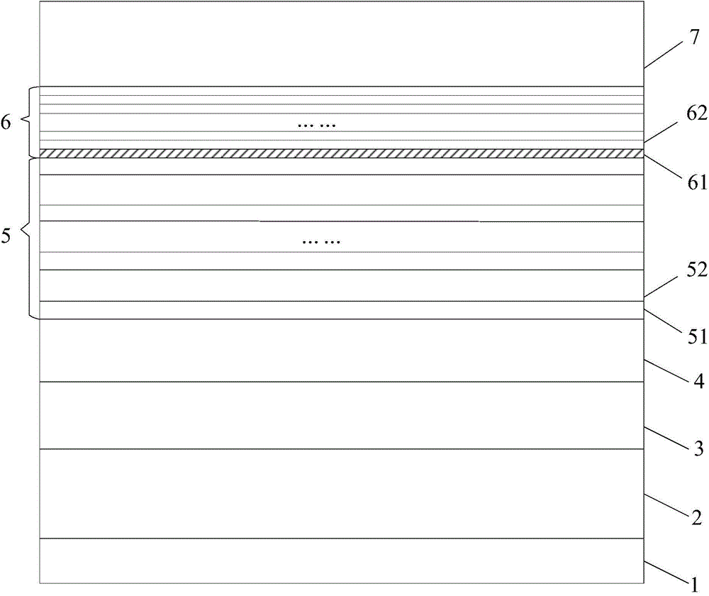
[0032] An embodiment of the present invention provides an LED epitaxial wafer, see figure 1 , the epitaxial wafer includes a substrate 1 , and a low-temperature buffer layer 2 , a high-temperature buffer layer 3 , an N-type layer 4 , an active layer 5 , an electron blocking layer 6 , and a P-type layer 7 sequentially stacked on the substrate 1 .

[0033] In this embodiment, the electron blocking layer 6 includes a GaN layer 61 ( figure 1 indicated by hatching), and at least two AlGaN layers 62 stacked on the GaN layer 61 in sequence. The Al composition content of the at least two AlGaN layers 62 increases or decreases layer by layer along the growth direction of the epitaxial wafer.

[0034] It should be noted that since the energy level height of the AlGaN layer energy band is related to the Al composition content, the Al composition content of at least two AlGaN layers 62 increases or decreases layer by layer along the growth direction of the epitaxial wafer, so at least tw...

Embodiment 2

[0061] An embodiment of the present invention provides a method for manufacturing an LED epitaxial wafer, which is used to manufacture the LED epitaxial wafer provided in Embodiment 1, see image 3 , the method includes:

[0062] Step 200: Perform pretreatment on the substrate.

[0063] In this embodiment, Veeco K465i type or C4 type MOCVD (Metal Organic Chemical Vapor Deposition, metal organic compound chemical vapor deposition) is used to realize the manufacturing method of the LED epitaxial wafer. Using high-purity H 2 (hydrogen) or high-purity N 2 (nitrogen) or high purity H 2 and high purity N 2 The mixed gas as the carrier gas, high-purity NH 3 As the N source, trimethylgallium (TMGa) and triethylgallium (TEGa) are used as the gallium source, trimethylindium (TMIn) is used as the indium source, silane (SiH4) is used as the N-type dopant, and trimethylaluminum ( TMAl) as an aluminum source, magnesium dicene (CP 2 Mg) as a P-type dopant.

[0064] Alternatively, the...


PUM


Abstract

The invention discloses an epitaxial wafer of a light emitting diode and a manufacturing method thereof and belongs to the technical field of semiconductors. The epitaxial wafer comprises an underlayer and a low temperature buffer layer, a high temperature buffer layer, an N type layer, an active layer, an electronic resisting layer and a P type layer which are stacked on the underlayer in sequence, wherein the electronic resisting layer comprises a GaN layer and at least two AlGaN layers stacked on the GaN layer; the Al component content of the AlGaN layers increases or reduces layer-by-layer in the growing direction of the epitaxial wafer. According to the invention, the electronic resisting layer is arranged, so that the energy level height of the electronic resisting layer increases or reduces layer-by-layer, the resisting function of injecting the active layer to a hole is weakened, electrons can be prevented from leaking from a quantum well, and the luminous efficiency is improved.

Description

technical field [0001] The invention relates to the technical field of semiconductors, in particular to a light-emitting diode epitaxial wafer and a manufacturing method thereof. Background technique [0002] LED (Light Emitting Diode, light-emitting diode) is a semiconductor electronic component that can emit light. It is widely used in traffic lights, outdoor full-color display screens, urban landscape lighting, automotive interior and exterior lights, and tunnel lights. [0003] High-power chips are LED chips with light source power greater than or equal to 350mw, and the specifications include 30mil*30mil, 45mil*45mil, 50mil*50mil, etc. Existing LED epitaxial wafers for manufacturing high-power chips include a substrate, and a low-temperature buffer layer, a high-temperature buffer layer, an N-type layer, an active layer, an electron blocking layer, and a P-type layer grown on the substrate in sequence. Wherein, the electron blocking layer is an AlGaN layer. [0004] I...

Claims


Application Information

Patent Timeline
Patent Type & Authority Applications(China)
IPC IPC(8): H01L33/14H01L33/12H01L33/00
CPCH01L33/0075H01L33/12H01L33/145
Inventor 从颖姚振韩杰胡加辉魏世祯
Owner HC SEMITEK SUZHOU
Why Eureka
Try Eureka