
X-waveband power amplifier based on GaN

A power amplifier and X-band technology, applied in the field of X-band power amplifiers, can solve the problems of increasing drain current, reducing output conductance, reducing device access resistance, etc., and achieving the effects of small voltage standing wave, low cost and stable operation

Inactive Publication Date: 2014-11-19
WUXI YANAO ELECTRONICS TECH
View PDF3 Cites 9 Cited by
  • Summary
  • Abstract
  • Description
  • Claims
  • Application Information

AI Technical Summary

Problems solved by technology

At present, the structure of HEMT is pseudomorphic GaAs HEMT, that is, a layer of InGaAs is added between AlGaAs / GaAs, which increases the channel electron mobility, increases the output current, and reduces the output conductance; double heterojunction HEMT, in A doped layer is introduced under the channel layer of the device, so that the channel produces a double-layer sheet-like carrier concentration. For a given device, the drain current will increase exponentially, and the access resistance of the device will be reduced. , also reduces the drain voltage that drives the device to saturation

Method used


Image

  • X-waveband power amplifier based on GaN
  • X-waveband power amplifier based on GaN
  • X-waveband power amplifier based on GaN

Examples


Embodiment Construction

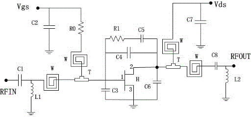
[0026] figure 1 It is a schematic diagram of the X-band GaN monolithic integrated power amplifier circuit. The circuit includes MIN capacitors, filter capacitors, film resistors, stable resistors, spiral inductors, microstrip transmission lines, T-shaped connectors, and GaN-based HEMTs. The signal input terminal (RFIN) is connected to the input terminal (1) of the GaN-based HEMT (H) through the first MIN capacitor (C1), microstrip transmission line (W), and T-junction (T), and the drain control terminal (Vds) Connect to the output terminal (2) of the GaN-based HEMT through a microstrip transmission line (W) and a T-shaped joint (T), the type of the microstrip transmission line (W) is a 100um high-impedance microstrip transmission line; the filter capacitor A 100uF electrolytic capacitor is selected, the model of the GaN-based HEMT (H) is NRF01-02a HEMT die, and the thin film resistor is made of NiCr material.

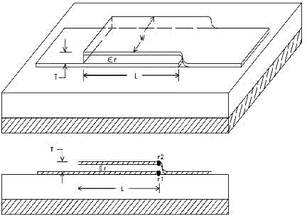
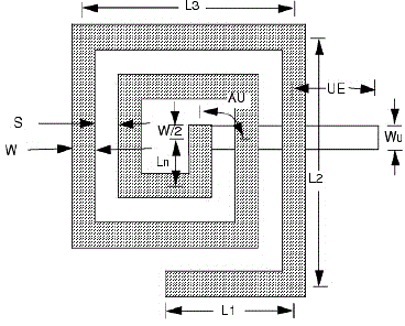
[0027] figure 2 It is the MIN capacitor structure diagram of th...


PUM


Abstract

The invention discloses an X-waveband power amplifier based on GaN. The X-waveband power amplifier comprises MIN capacitors, a filter capacitor, a thin-film resistor, a stable resistor, a spiral inductor, a microstrip transmission line, a T-shaped connector and a GaN-based HEMT. A signal input end (RFIN) is connected with an input end (1) of the GaN-based HEMT (H) through the first MIN capacitor (C1), the microstrip transmission line (W) and the T-shaped connector (T). A drain electrode control end (Vds) is connected with an output end (2) of the GaN-based HEMT through the microstrip transmission line (W) and the T-shaped connector (T). The microstrip transmission line (W) is a 100-micrometer high-impedance microstrip transmission line. A 100-microfarad electrolytic capacitor is selected as the filter capacitor. The GaN-based HEMT (H) is an NRF01-02a HEMT tube core. The thin-film resistor is made of NiCr material. The X-waveband power amplifier is matched with the input end in a conjugate mode through a load traction method so as to solve the problem that negative resistance occurs at the port of the transistor; the X-waveband power amplifier is stable in work, has the bandwidth of 3.6 GHz to 8.0 GHz, the maximum gain of 11.04 dB, the maximum output power of 33 dBm and the maximum PAE of 29.2%, and is small in voltage standing wave ratio.

Description

technical field [0001] The invention belongs to the field of power electronics application technology, in particular to a GaN-based X-band power amplifier. Background technique [0002] High Electron Mobility Transistor (HEMT) is a research hotspot of power devices in recent years, and its working principle is similar to MESFET. HEMT uses a vertical structure, uses multiple layers of different materials, and selects different materials to form the conduction channel of the device, so that the electrons in the channel are separated from the donor atoms in space. The scattering of ion impurities is reduced and the electron mobility is improved. Through the material doping and the physical and chemical properties between the materials of each layer, a narrow channel with a high electron concentration is formed between the source and the drain, thereby making a device with high output current. At present, the structure of HEMT is pseudomorphic GaAs HEMT, that is, a layer of I...

Claims


Application Information

Patent Timeline
Patent Type & Authority Applications(China)
IPC IPC(8): H03F3/20H03F1/34
Inventor 唐余武邹明炳邹坤
Owner WUXI YANAO ELECTRONICS TECH
Learn More