Vertical GaN heterojunction field-effect transistor with P type GaN island

A heterojunction field effect, GaN-based technology, applied in semiconductor devices, electrical components, circuits, etc., to achieve the effects of reducing drain leakage current, increasing electric field strength, and improving withstand voltage strength

Active Publication Date: 2014-11-26
UNIV OF ELECTRONICS SCI & TECH OF CHINA
View PDF3 Cites 13 Cited by
  • Summary
  • Abstract
  • Description
  • Claims
  • Application Information

AI Technical Summary

Problems solved by technology

However, the electric field between the source and drain of this structure presents a zigzag distribution, and when the electric field at the interface of each p-n junction reaches the critical electric field, the electric field at other positions is still lower than the critical breakdown electric field, and the withstand voltage still has the potential to be further improved.

Method used


Image

  • Vertical GaN heterojunction field-effect transistor with P type GaN island
  • Vertical GaN heterojunction field-effect transistor with P type GaN island
  • Vertical GaN heterojunction field-effect transistor with P type GaN island

Examples


Embodiment 1

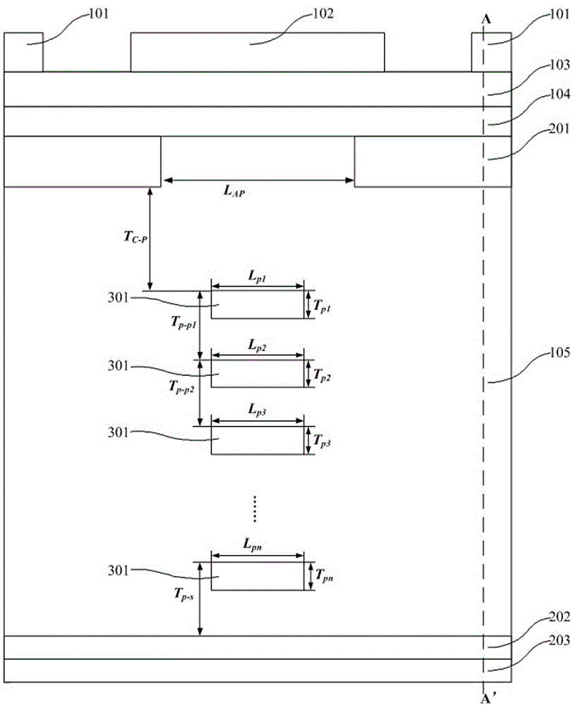
[0030] The main structure of this embodiment, such as image 3 As shown, it includes a barrier layer 103, the upper part of the barrier layer 103 is provided with a source 101 and a gate 102, and the lower part is a channel layer 104, a p-GaN current blocking layer 201, an n-GaN buffer layer 105, n + -GaN substrate 202, drain 203, the center of the p-GaN current blocking layer 201 is provided with a width L AP aperture, and nested in the upper part of the n-GaN buffer layer 105, the n-GaN buffer layer 105 is provided with a p-GaN island 301, and the p-GaN island 301 is located between the p-GaN current blocking layer 201 and the n + - between GaN substrates 202 .

[0031] Wherein, the p-GaN island 301 is divided into n layers from top to bottom along the longitudinal axis, where n is a positive integer, and the range of n is 1≤n≤1000.

[0032] Each layer of the p-GaN island layer 301 has the same centerline, which is also the centerline of the n-GaN buffer layer 105 .

[00...


PUM


Abstract

The invention discloses a vertical GaN heterojunction field-effect transistor with a P type GaN island. The field-effect transistor comprises an AlGaN barrier layer, wherein a source electrode and a grid electrode are arranged on the AlGaN barrier layer, and a GaN channel layer, a p-GaN current blocking layer, an n-GaN buffer layer, an n+-GaN substrate and a drain electrode are arranged under the AlGaN barrier layer in sequence. A hole with the caliber of LAP is formed in the center of the p-GaN current blocking layer and nested to the n-GaN buffer layer, the p-GaN island is arranged in the n-GaN buffer layer, and the p-GaN island is located between the p-GaN current blocking layer and the n+-GaN substrate. In the GaNPI-VHFET, by using the p-GaN island layer, extra p type impurities are introduced into the n-GaN buffer layer, and the n-GaN buffer layer area is exhausted in the off state, so that the buffer area is equivalent to an intrinsic region during voltage resistance. Therefore, the problem that the vertical electric field intensity is continuously decreased when current moves far away from an interface of the p-GaN current blocking layer and the n-GaN buffer layer is solved to increase breakdown voltage of a device. Meanwhile, leaked current of the drain electrode is also decreased in the off state.

Description

technical field [0001] The invention relates to the field of semiconductor high withstand voltage devices, in particular to a vertical GaN-based heterojunction field effect transistor with P-type GaN islands. Background technique [0002] Gallium nitride-based heterojunction field effect transistor (GaN Heterojunction Fiele-Effect Transistor, GaN HFET) not only has a large band gap, high critical breakdown electric field, high electron saturation velocity, good thermal conductivity, radiation resistance and good chemical stability At the same time, gallium nitride (GaN) materials can form a two-dimensional electron gas heterojunction channel with high concentration and high mobility with materials such as aluminum gallium nitride (AlGaN), so it is especially suitable for high-voltage, high-power And high temperature applications, it is one of the most potential transistors for power electronics applications. [0003] The existing high withstand voltage GaN HFET structure is...

Claims


Application Information

Patent Timeline
Patent Type & Authority Applications(China)
IPC IPC(8): H01L29/778H01L29/06
CPCH01L29/0603H01L29/7788
Inventor 杜江锋刘东陈南庭潘沛霖于奇
Owner UNIV OF ELECTRONICS SCI & TECH OF CHINA
Why Eureka
Try Eureka