LED flip chip and patterned substrate and manufacturing method of LED flip chip

A patterned substrate, flip-chip technology, applied in electrical components, circuits, semiconductor devices, etc., can solve problems such as increasing device heat transfer, device efficiency, adverse effects on performance parameters and reliability, and reducing device external quantum efficiency. , to increase the probability of exit, improve brightness and electro-optical conversion efficiency, and increase the efficiency of light extraction

Inactive Publication Date: 2014-12-03
江苏鑫博电子科技有限公司
View PDF8 Cites 3 Cited by
  • Summary
  • Abstract
  • Description
  • Claims
  • Application Information

AI Technical Summary

Problems solved by technology

Therefore, it is necessary to pattern the surface of the substrate material to improve the light extraction efficiency and minimize the reduction of device efficiency due to total reflection.
[0004] Taking GaN-based blue LED epitaxial growth in the direction of SiC (0001) crystal plane and making flip chip as an example, since more light is to be emitted from the substrate surface (the side where the epitaxial growth is not performed), the light from The total reflection angle of SiC incident into the air is only about 22 degrees (the refractive index of SiC is 2.7, and the air is 1.0), so it is necessary to roughen or pattern the surface of the substrate, otherwise, from the active area It will be difficult for the recombined photons to escape from the device, and the external quantum efficiency of the device will be significantly reduced
At the same time, since the generated photons cannot be effectively extracted, the heat conversion of the device will be increased, which will further adversely affect the quality characteristics of the device such as efficiency, performance parameters and reliability.

Method used


Image

  • LED flip chip and patterned substrate and manufacturing method of LED flip chip
  • LED flip chip and patterned substrate and manufacturing method of LED flip chip
  • LED flip chip and patterned substrate and manufacturing method of LED flip chip

Examples


Embodiment 1

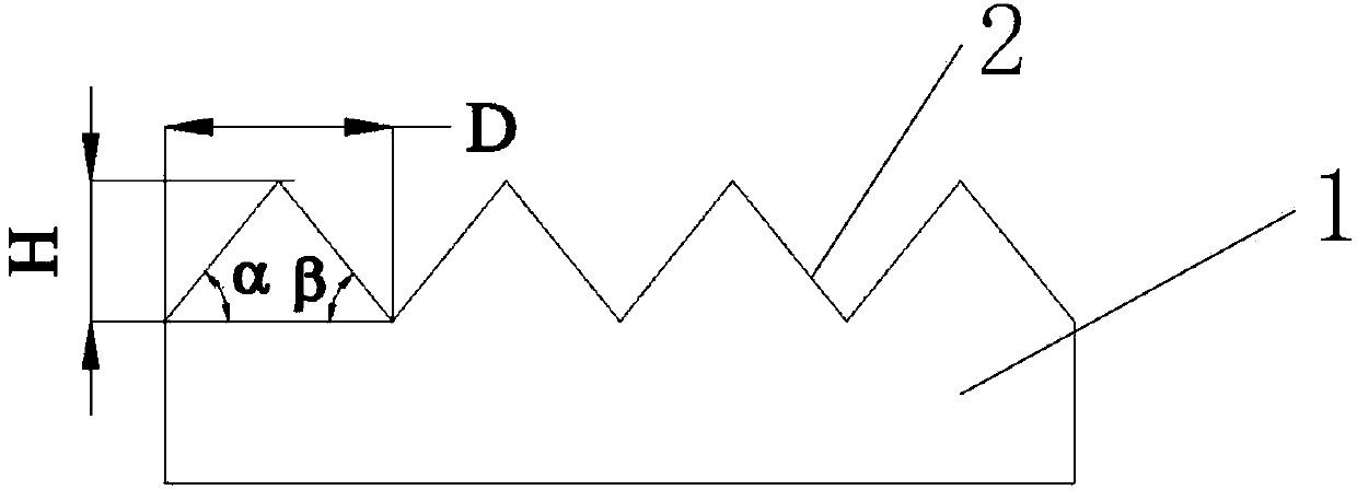
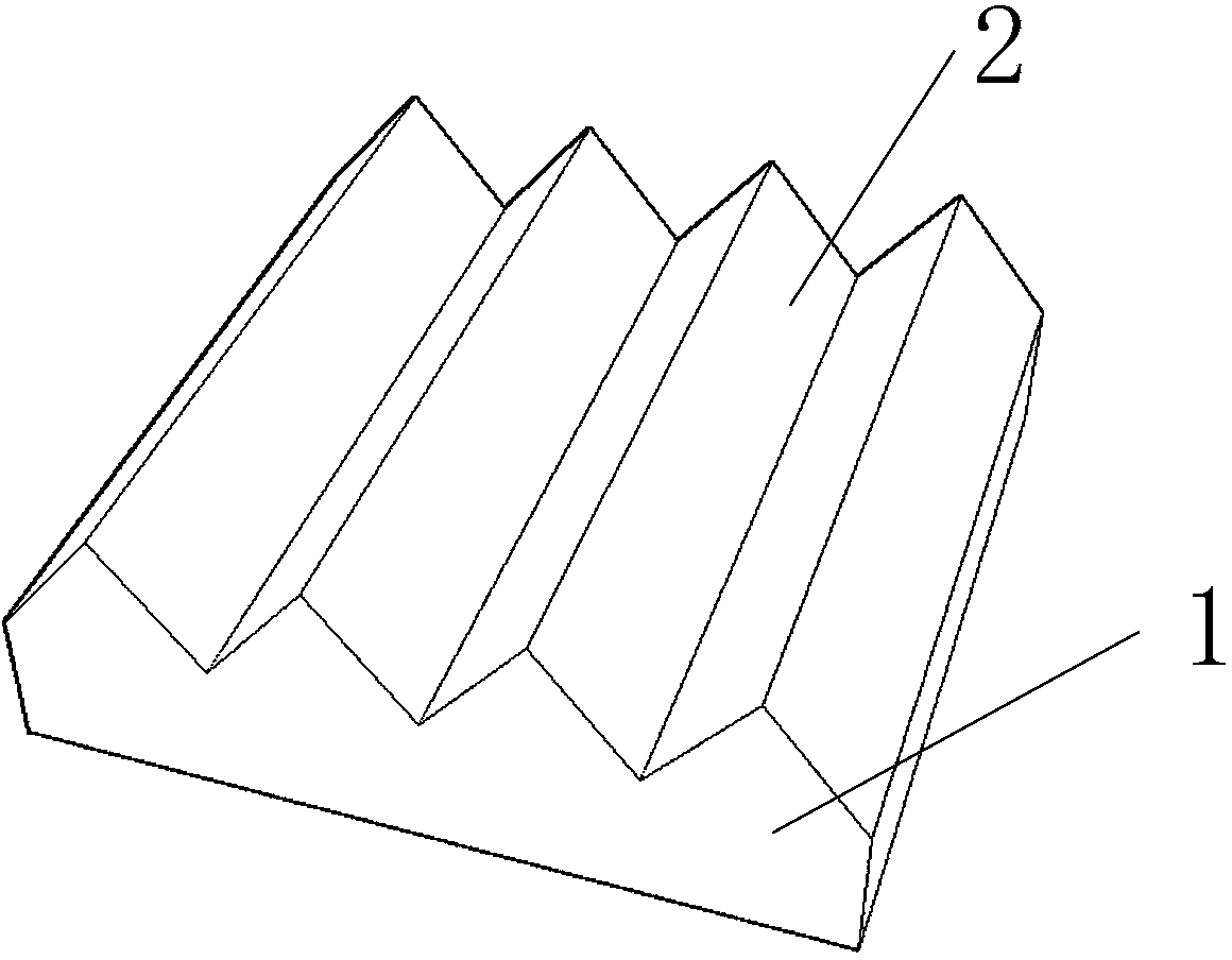
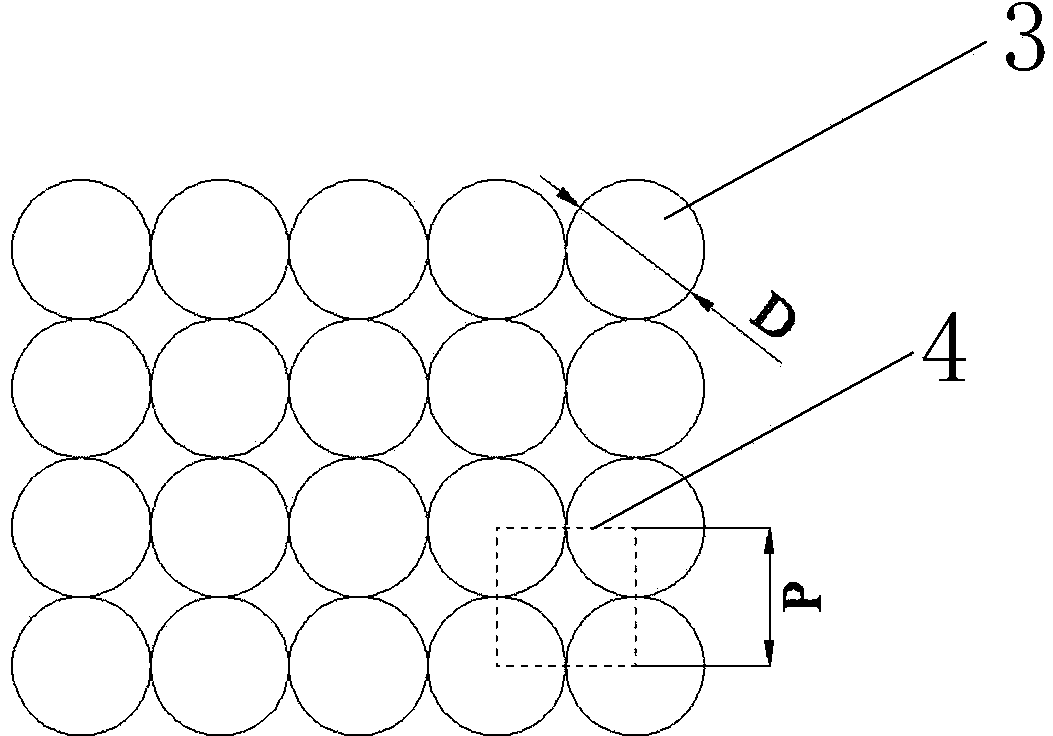
[0041] A patterned substrate for LED flip chips. The surface of the patterned substrate 1 is provided with grooves 2 with a triangular cross-section and parallel to each other, or provided with a plurality of convex structures 3 arranged in regular shapes. Graphics Array4.

[0042] The triangular cross-section is preferably an isosceles triangle, and the base angle of the triangular cross-section ranges from 10 to 80 degrees. The width of the trench 2 ranges from 10 nm to 200 μm. The graphic array 4 is arranged in a rectangular or hexagonal close-packed array, and the side length of the rectangular and hexagonal close-packed arrays ranges from 10 nm to 50 μm.

[0043] The shape of the protruding structure 3 is one or more of a cone, a cone-like body, a regular polygonal pyramid, a hemisphere, a spherical segment, a cylinder, and a regular polyhedron.

[0044] The size of the bottom of the raised structures 3 ranges from 10 nm to 50 μm; the height of each raised structure 3 ran...


PUM


Abstract

The invention relates to an LED flip chip and a patterned substrate and manufacturing method of the LED flip chip. The surface of the patterned substrate is provided with grooves or a pattern array, wherein the cross sections of the grooves are triangular, the grooves are parallel to one another, and the pattern array is composed of protrusion structures which are arranged to form a regular shape. The LED flip chip comprises the patterned substrate, an epitaxial layer, P electrodes and N electrodes. The patterned substrate is arranged on the upper surface of the epitaxial layer. The P electrodes and the N electrodes are respectively arranged on the lower surface of the epitaxial layer. By means of the LED flip chip, the patterned substrate and the manufacturing method, the probability that photons are emitted out of the chip can be increased, and in other words, the light ray extraction efficiency of devices is increased so that the brightness of LEDs and the electro-optical conversion efficiency can be improved.

Description

technical field [0001] The invention relates to the technical field of manufacturing LED optoelectronic devices, in particular to an LED flip chip, a patterned substrate of the LED flip chip and a manufacturing method. Background technique [0002] Using Al Arsenide x In y Ga 1-x-y As(0≤x,y≤1; x+y≤1), phosphide Al x In y Ga 1-x-y P(0≤x,y≤1; x+y≤1), nitride Al x In y Ga 1-x-y N (0≤x, y≤1; x+y≤1; wurtzite crystal structure) light-emitting diode LEDs made of semiconductor materials are gradually being used in electronic display screens, landscape lighting, miner's lamps, and street lamps due to their advantages in energy saving, environmental protection, and long life. , liquid crystal display backlight, general lighting, optical disc information storage, biomedicine and other fields are widely used. The above-mentioned compound semiconductors can cover the entire spectral energy range from infrared, visible to ultraviolet light, and the emission wavelength of LED devi...

Claims


Application Information

Patent Timeline
Patent Type & Authority Applications(China)
IPC IPC(8): H01L33/20H01L33/32H01L33/00
CPCH01L33/20H01L33/0075H01L33/32
Inventor 马亮李金权刘素娟裴晓将胡兵
Owner 江苏鑫博电子科技有限公司
Why Eureka
Try Eureka