Forming method of conductive plug

A technology of conductive plugs and conductive materials, applied in the direction of circuits, electrical components, electrical solid devices, etc., can solve the problems of easy collapse, poor etch resistance, low yield, etc., and achieve good appearance, high etch resistance, The effect of high yield

Active Publication Date: 2014-12-17
SEMICON MFG INT (SHANGHAI) CORP
View PDF9 Cites 7 Cited by
  • Summary
  • Abstract
  • Description
  • Claims
  • Application Information

AI Technical Summary

Problems solved by technology

However, when the thicker low temperature oxide layer 2 is used as a mask, part of the low temperature oxide 21 between the two openings 20 will have a tall and thin (slim) cross-sectional shape, and the part of the low temperature oxide 21 itself is easy to Collapse, especially in the case of continuous shrinking of the feature size of semiconductor devices, the distance between the two openings 20 is getting smaller and smaller, and this collapse phenomenon is more likely to occur
More seriously, as mentioned above, in the process of etching the dielectric layer 1 to form a contact hole (not shown), the low temperature oxide layer 2 is also continuously etched. Although the plasma etching is anisotropic etching, the During the etching process, the side of the part of the low-temperature oxide 21 will inevitably be slightly etched, but due to the poor etch resistance of the low-temperature oxide layer 2 under plasma etching conditions, even a slight etching may make part of the low-temperature oxide 21 become thinner, thus further increasing the possibility of the collapse of the part of the low temperature oxide 21
Once the part of the low-temperature oxide 21 collapses, it will lead to poor morphology of the formed contact hole (not shown), and finally lead to a low yield of the formed conductive plug.
Therefore, there is an urgent need for a method for forming conductive plugs to solve the problem of low yield in existing methods for forming conductive plugs

Method used


Image

  • Forming method of conductive plug
  • Forming method of conductive plug
  • Forming method of conductive plug

Examples


Embodiment Construction

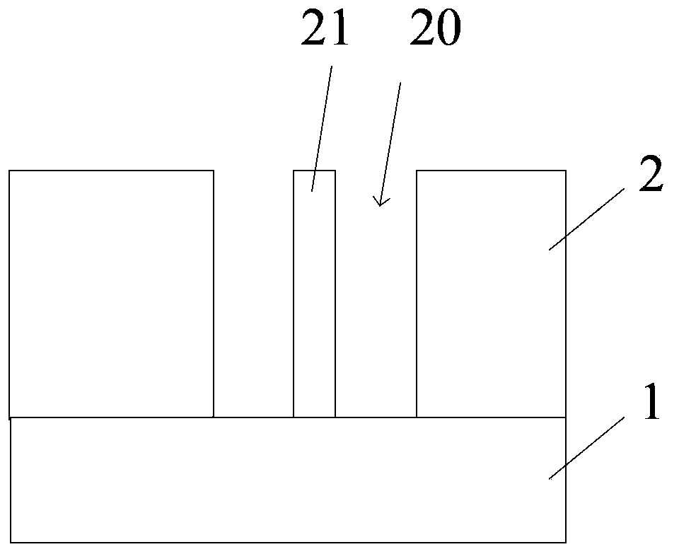
[0040] It can be known from the background art that in the conventional method for forming a conductive plug, a relatively thick low temperature oxide layer needs to be used as a mask. However, the use of a thicker low temperature oxide layer tends to result in a low yield of formed conductive plugs.

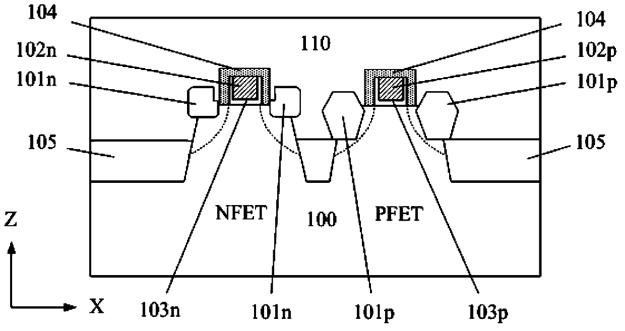
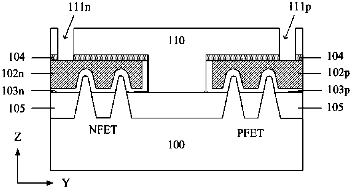
[0041] Taking the fin field effect transistor in the prior art as an example, the distance between the source region and the drain region on the same fin field effect transistor is getting smaller and smaller, although the gate region contact holes can be arranged on the gates on both sides of the fin part. Therefore, the distance between the contact holes in the gate region is relatively large, that is, the contact holes in the gate region can use a low temperature oxide layer as a mask. However, when the low temperature oxide layer is used as a mask to form the source contact holes and the drain contact holes, it is easy to cause the low temperature oxide layer to collapse, so...


PUM


Abstract

A forming method of a conductive plug includes: providing a semiconductor substrate which is provided with transistors and a medium area covering the transistors, wherein each transistor comprises a source drain area and a grid area; forming a hard mask layer on the medium layer; forming openings corresponding drain source areas in the hard mask layer; using the residual hard mask as a mask to etch the medium layer along the openings until the source drain area contact holes of the source drain areas are exposed; allowing the source drain area contact holes to be filled with conductive materials. The forming method has the advantages that the hard mask layer is high in etching resistance and small in thickness, the contact holes formed by using the hard mask layer as the mask are good in morphology, and the finally formed conductive plug is high in yield.

Description

technical field [0001] The present invention relates to the field of semiconductor technology, in particular to a method for forming a conductive plug. Background technique [0002] With the development of integrated circuits to ultra-large-scale integration (ULSI), the feature size of semiconductor devices continues to shrink. In this process, traditional field-effect transistors (Field-Effect Transistor, FET) face increasingly serious short-channel effects and reliability degradation. As a result, the industry has developed a fin field effect transistor (FinFET). The double gate or half gate of the FinFET can suppress the short-channel effect, and can improve the gate control capability and improve the reliability of the transistor. [0003] However, the fabrication process of FinFET is not very mature, especially when making conductive plugs of FinFET, there are difficulties. [0004] Please refer to figure 1 In the existing fabrication method of FinFET, a low temperat...

Claims


Application Information

Patent Timeline
Patent Type & Authority Applications(China)
IPC IPC(8): H01L21/337
CPCH01L21/0332H01L21/76805H01L21/76816H01L29/66795H01L2221/101
Inventor 张海洋张城龙
Owner SEMICON MFG INT (SHANGHAI) CORP
Why Eureka
Try Eureka