

Solar cell antireflection film and manufacturing method thereof
A technology of solar cells and anti-reflection films, applied in circuits, photovoltaic power generation, electrical components, etc., can solve the problem that the anti-reflection effect and passivation effect of thin films cannot be taken into account at the same time, achieve good passivation effect and anti-reflection effect, improve Good conversion efficiency and anti-reflection effect
- Summary
- Abstract
- Description
- Claims
- Application Information
AI Technical Summary
Problems solved by technology
Method used
Image

Examples
preparation example Construction
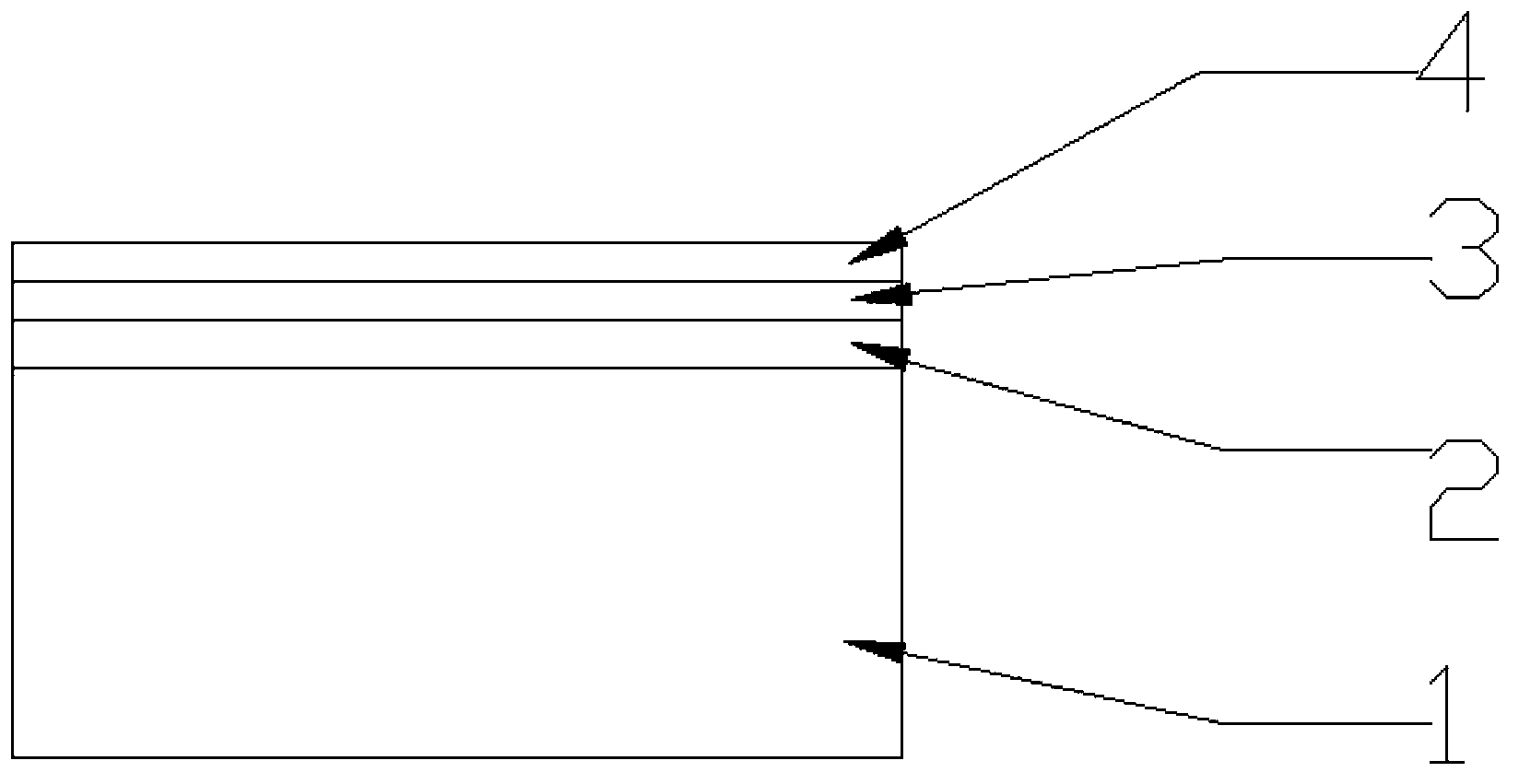
[0023] The present invention also provides a method for preparing an anti-reflection film, comprising the following steps:
[0024] a) placing the etched solar cell silicon wafer in a plasma-enhanced chemical vapor deposition device, and feeding silane and hydrogen gas to deposit an amorphous silicon layer on the surface of the solar cell silicon wafer;
[0025] b) passing silane and ammonia gas into the plasma-enhanced chemical vapor deposition equipment to deposit a first silicon nitride film on the surface of the amorphous silicon layer;
[0026] c) Continue to feed silane and ammonia gas into the plasma enhanced chemical vapor deposition equipment to deposit a second silicon nitride film on the surface of the amorphous silicon layer.
[0027] Before coating the silicon wafers of crystalline silicon solar cells, the silicon wafers need to be processed. The specific process is as follows:
[0028] The silicon wafer is cleaned and corroded for texturing, and then the silicon...
Embodiment 1
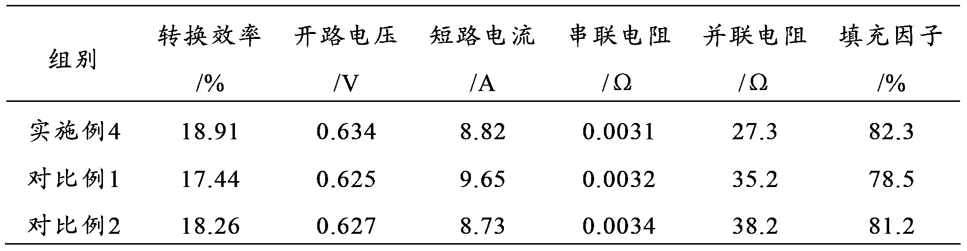
[0036] 600 pieces of P-type polysilicon wafers produced by JinkoSolar Holding Co., Ltd. were used, the resistivity of which was 0.5Ω·cm~3Ω·cm, and the thickness of the silicon wafers was 200±20μm. 600 pieces of silicon wafers were cleaned and etched to make texture, and the thinning amount of silicon wafers was controlled to 0.4g~0.5g; then 600 pieces of silicon wafers were put into the diffusion furnace to diffuse 200 pieces at a time, and divided into three times in a furnace tube Medium diffusion, the square resistance is controlled to 60~70Ω / □; after plasma etching and dephosphorous silicon glass. The 600 pieces of phosphorus-silicate glass after removal were divided into six batches, each batch of 100 pieces was marked as the first batch, the second batch, the third batch, the fourth batch, the fifth batch and the sixth batch.
Embodiment 2
[0038] 1) Place the first batch of silicon wafers in the deposition chamber of the tubular PECVD coating equipment. The deposition temperature is 200°C, the deposition power is 50W, and silane with a gas flow rate of 30min / L and a flow rate of 60L / min are introduced into the furnace tube. Hydrogen gas, the working gas voltage is 80-100Pa, the RF power frequency is 13.46MHz, and after 1min, a layer of amorphous silicon layer with a film thickness of 30nm is deposited on the surface of the silicon wafer;
[0039] 2) Continue to deposit the silicon wafer coated with amorphous silicon layer, feed silane with a gas flow rate of 40min / L and ammonia gas with a gas flow rate of 120min / L into the furnace tube, the substrate temperature is 500°C, and the RF power is 6000W, the gas pressure is 300Pa, after a duration of 1min, a first silicon nitride film is deposited on the surface of the amorphous silicon layer, the film thickness of the first silicon nitride film is 40nm, and the refrac...
PUM
| Property | Measurement | Unit |
|---|---|---|
| thickness | aaaaa | aaaaa |
| thickness | aaaaa | aaaaa |
| thickness | aaaaa | aaaaa |
Abstract
Description
Claims
Application Information