Bi-directional light control thyratron transistor chip, optical triggering coupler and solid-state relay

A thyristor, bidirectional light technology, applied in semiconductor devices, circuits, electrical components, etc., can solve the problem of increasing the chip area, achieve the effect of improving the rectification characteristics and suppressing the increase of the chip area

Active Publication Date: 2014-12-24
SHARP KK
View PDF3 Cites 0 Cited by
  • Summary
  • Abstract
  • Description
  • Claims
  • Application Information

AI Technical Summary

Problems solved by technology

[0031] As can be seen from the above, in the conventional bidirectional phototriac thyristor disclosed in the above-mentioned Patent Document 1, there is a problem that the chip area becomes large.

Method used


Image

  • Bi-directional light control thyratron transistor chip, optical triggering coupler and solid-state relay
  • Bi-directional light control thyratron transistor chip, optical triggering coupler and solid-state relay
  • Bi-directional light control thyratron transistor chip, optical triggering coupler and solid-state relay

Examples


no. 1 approach

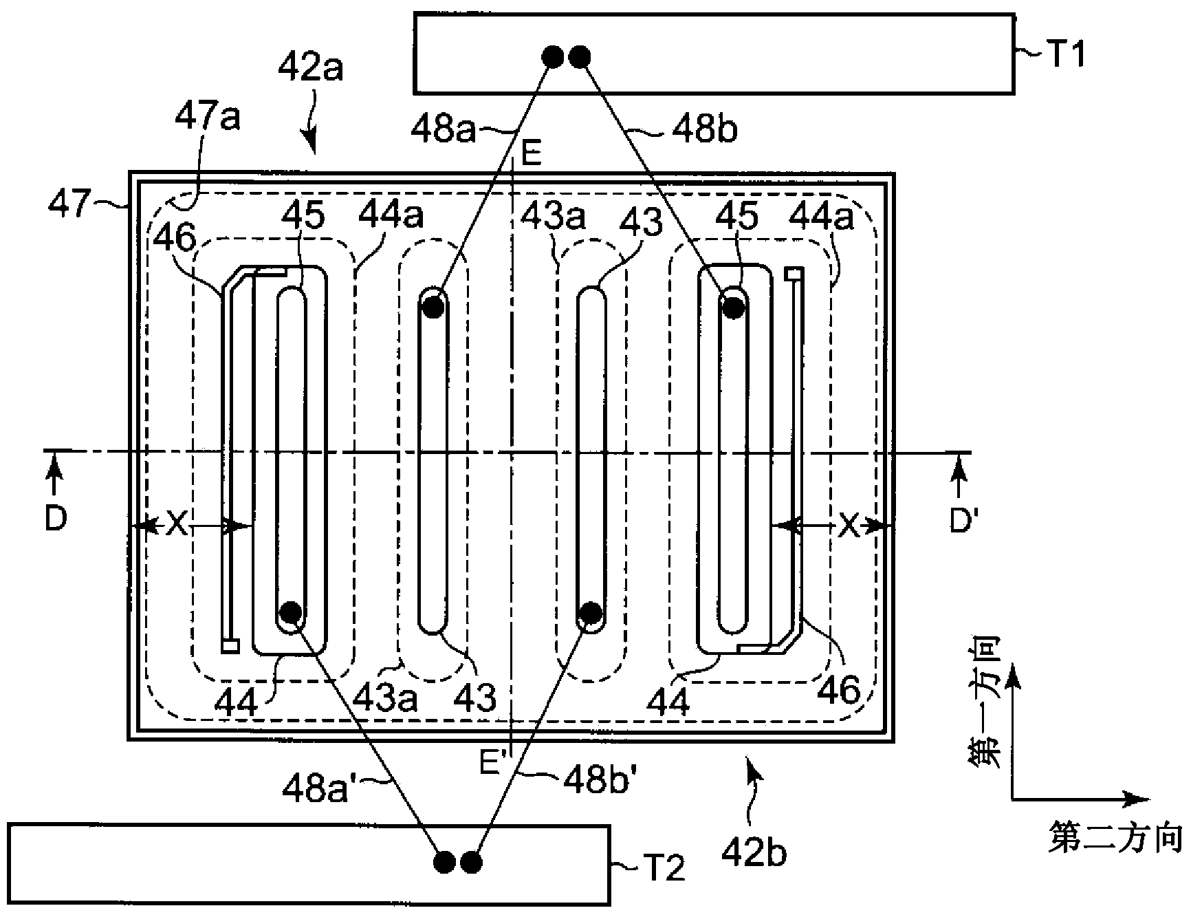
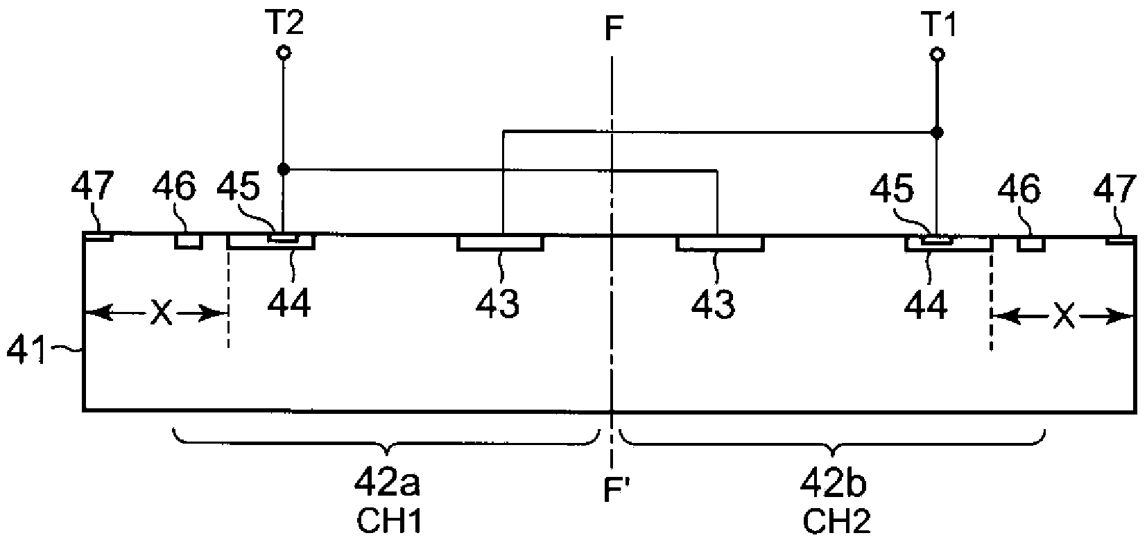
[0109] figure 1 A schematic pattern layout of the bidirectional phototriac thyristor chip of the present embodiment is shown, figure 2 yes figure 1 The schematic diagram of the D-D' cross-section.

[0110] The bidirectional light-controlled thyristor chip of this embodiment, such as figure 1 and figure 2 As shown, it includes: the first photothyristor 42a of CH1 and the second photothyristor 42b of CH2 formed separately on the surface of the N-type silicon substrate 41 constituting the chip.

[0111] The above-mentioned first photo-controlled thyristor 42a and the second photo-controlled thyristor 42b each have: a P-type anode diffusion region 43; a P-type gate diffusion region 44 opposite to the anode diffusion region 43; An N-type cathode diffusion region 45 is formed in the electrode diffusion region 44 to face the anode diffusion region 43 . In this way, a PNPN portion is formed from the anode diffusion region 43 to the cathode diffusion region 45 . In addition,...

no. 2 approach

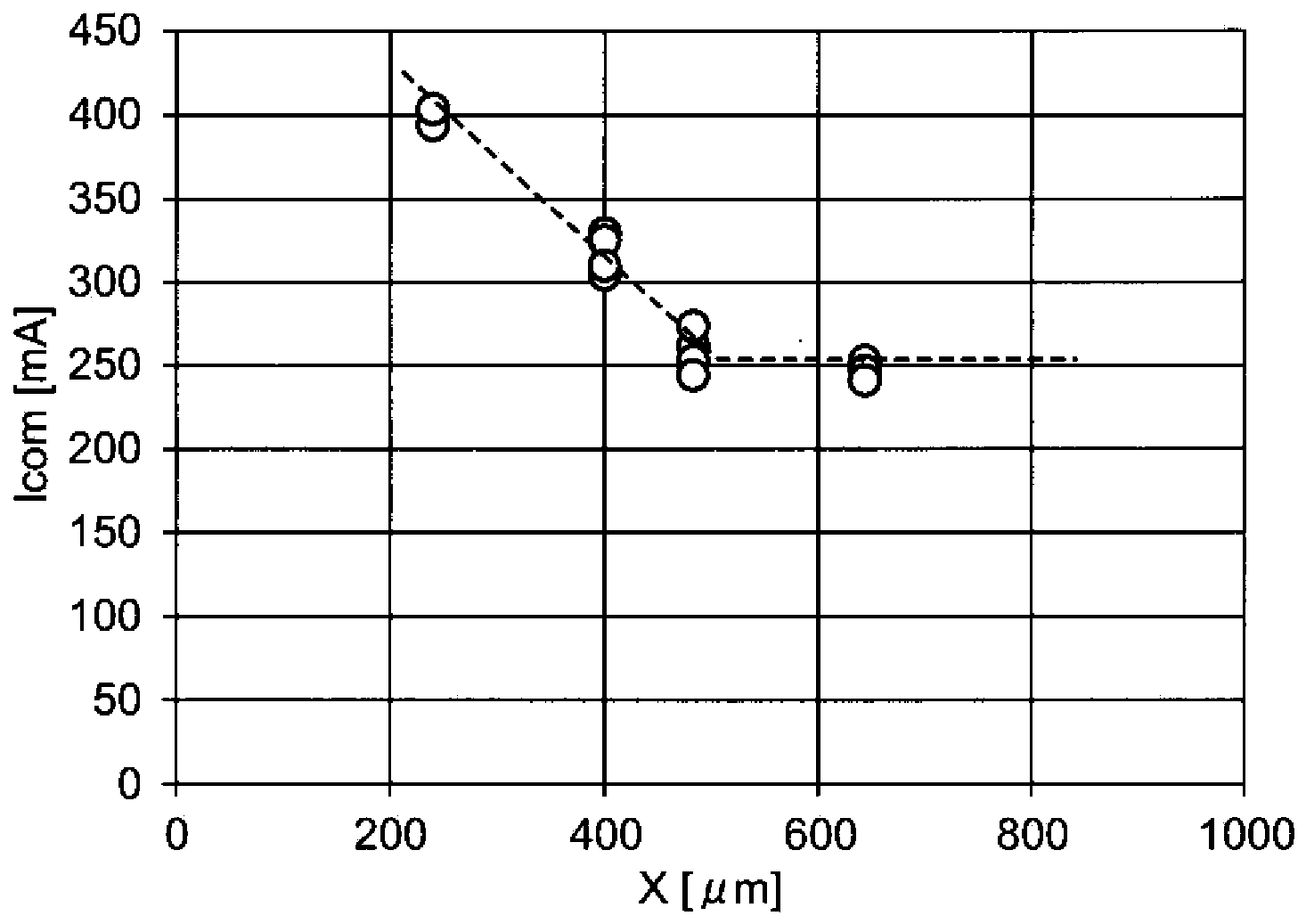
[0134] This embodiment relates to the "critical turn-off voltage rise rate dV / dt (hereinafter referred to simply as dV / dt characteristic)" and the "rectification characteristic Icom" and " Photosensitivity IFT".

[0135] Here, the aforementioned dV / dt characteristics and photosensitivity IFT will be described.

[0136] The above-mentioned "dV / dt characteristic" is determined by the minimum rising edge (=dV / dt) of the false conduction of the bidirectional phototronic thyristor when a pulse voltage with a steep rising edge is applied to the bidirectional phototronic thyristor. definition. This dV / dt characteristic represents noise tolerance. Therefore, it can be said that the larger the dV / dt characteristic is, the better it is in terms of high noise tolerance.

[0137] On the other hand, photosensitivity is used for example in Figure 22 In the light trigger coupler 3 shown, the minimum forward current value IFT when the forward current IF flows through the light emitting e...

no. 3 approach

[0170] The present embodiment relates to the gap Z1 between the high-concentration P-type diffusion region constituting the short diode as the channel separation region and the anode diffusion region.

[0171] Figure 14 It is a schematic cross-sectional view of the bidirectional phototriac thyristor chip of this embodiment. The basic structure of the bidirectional photo-controlled thyristor chip of this embodiment is the same as figure 1 and figure 2 The diac chip shown is the same. Figure 14 with the first embodiment described above figure 2 correspond. Thus, in Figure 14 In the bidirectional photo-controlled thyristor chip shown, in order to facilitate understanding, the figure 1 and figure 2 The components that are the same as those shown in the bidirectional photo-controlled thyristor chips are marked with the same symbols, and detailed descriptions are omitted.

[0172] In this embodiment, in addition to the structure of the bidirectional photothyristor ch...


PUM


Abstract

The invention provides a bi-directional light control thyratron transistor chip, an optical triggering coupler and a solid-state relay. A first light control thyratron transistor section and a second light control thyratron transistor section are arranged on a surface of a semiconductor chip. Each light control thyratron transistor section has a PNPN section. The PNPN section comprises a positive electrode diffusion region in a conductive type, a substrate in another conductive type, a control electrode diffusion region in a conductive type and a negative electrode diffusion region formed in the control electrode diffusion region in another conductive type. The distance of the cut surface to the control electrode diffusion region is below 400 micrometers. Thus, a few of minority carriers generated at the first light control thyratron transistor section side during connection are collected to the cut surface at the first light control thyratron transistor section side before migration. Schottky barrier or a channel separation region cannot be formed, rectification characteristics are raised greatly, increase of the chip area can be inhibited and load is controlled through light triggering by one chip.

Description

technical field [0001] The present invention relates to a bi-directional photothyristor chip (bi-directional photothyristor chip), a trigger coupler using the above-mentioned bi-directional photothyristor chip, and a solid-state relay (hereinafter referred to as SSR) using the above-mentioned trigger coupler . Background technique [0002] For a long time, as an SSR used under communication, there are such Figure 21 The circuit configuration shown is the SSR. The SSR8 includes: an optical trigger coupler 3 including light-emitting elements 1 such as LEDs (light-emitting diodes) and a triggering bidirectional photo-controlled thyristor 2; a bi-directional thyristor (hereinafter also referred to as case of the main thyristor) 4; and a snubber circuit (snubber circuit) 7 including a resistor 5, a capacitor 6, and the like. [0003] In addition, the equivalent circuit diagram of the optical trigger coupler 3 constituting the above-mentioned SSR8 is as follows: Figure 22 sho...

Claims


Application Information

Patent Timeline
Patent Type & Authority Applications(China)
IPC IPC(8): H01L31/111H01L31/0352H01L31/18H03K17/78
CPCH01L31/035272H01L31/1113H01L31/125H01L31/1804Y02P70/50
Inventor 一条尚生鞠山满
Owner SHARP KK
Why Eureka
Try Eureka