Solder bump and forming method therefor, and substrate having solder bump and manufacturing method for substrate having solder bump

A technology of solder bumps and substrates, which is applied to substrates with solder bumps and its manufacture, and the field of substrates with solder bumps and its manufacture, which can solve problems such as disappearance of copper patterns, achieve good dimensional accuracy, prevent defects or disappearance, The effect of ensuring reliability

Active Publication Date: 2014-12-24
TANIGUROGUMI CORP
View PDF6 Cites 11 Cited by
  • Summary
  • Abstract
  • Description
  • Claims
  • Application Information

AI Technical Summary

Problems solved by technology

However, when the mounting substrate is directly dipped in molten solder, the tin contained in the solder dissolves the copper of the copper electrode to cause so-called "copper dissolution", and there is a problem that the copper pattern disappears.

Method used


Image

  • Solder bump and forming method therefor, and substrate having solder bump and manufacturing method for substrate having solder bump
  • Solder bump and forming method therefor, and substrate having solder bump and manufacturing method for substrate having solder bump
  • Solder bump and forming method therefor, and substrate having solder bump and manufacturing method for substrate having solder bump

Examples


Embodiment 1

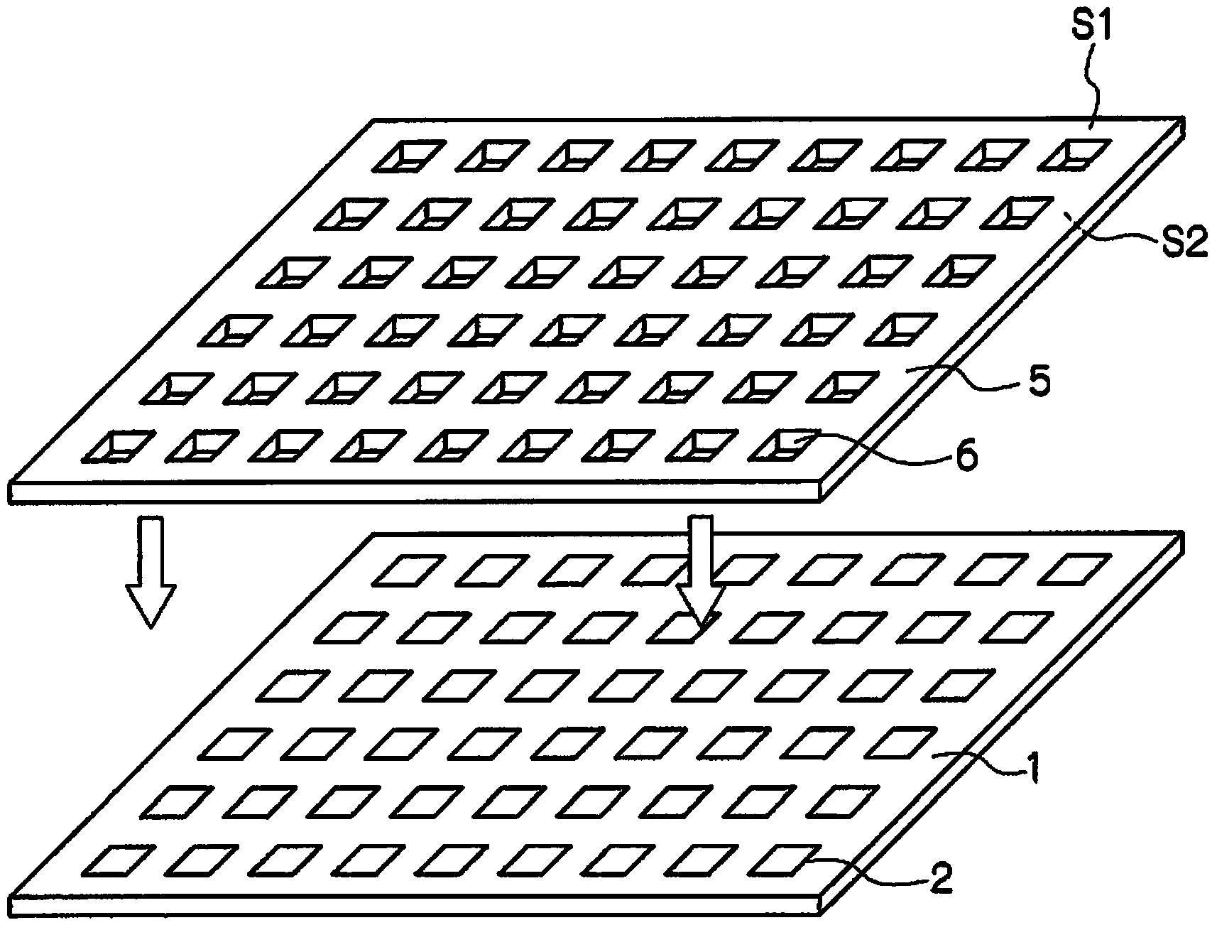
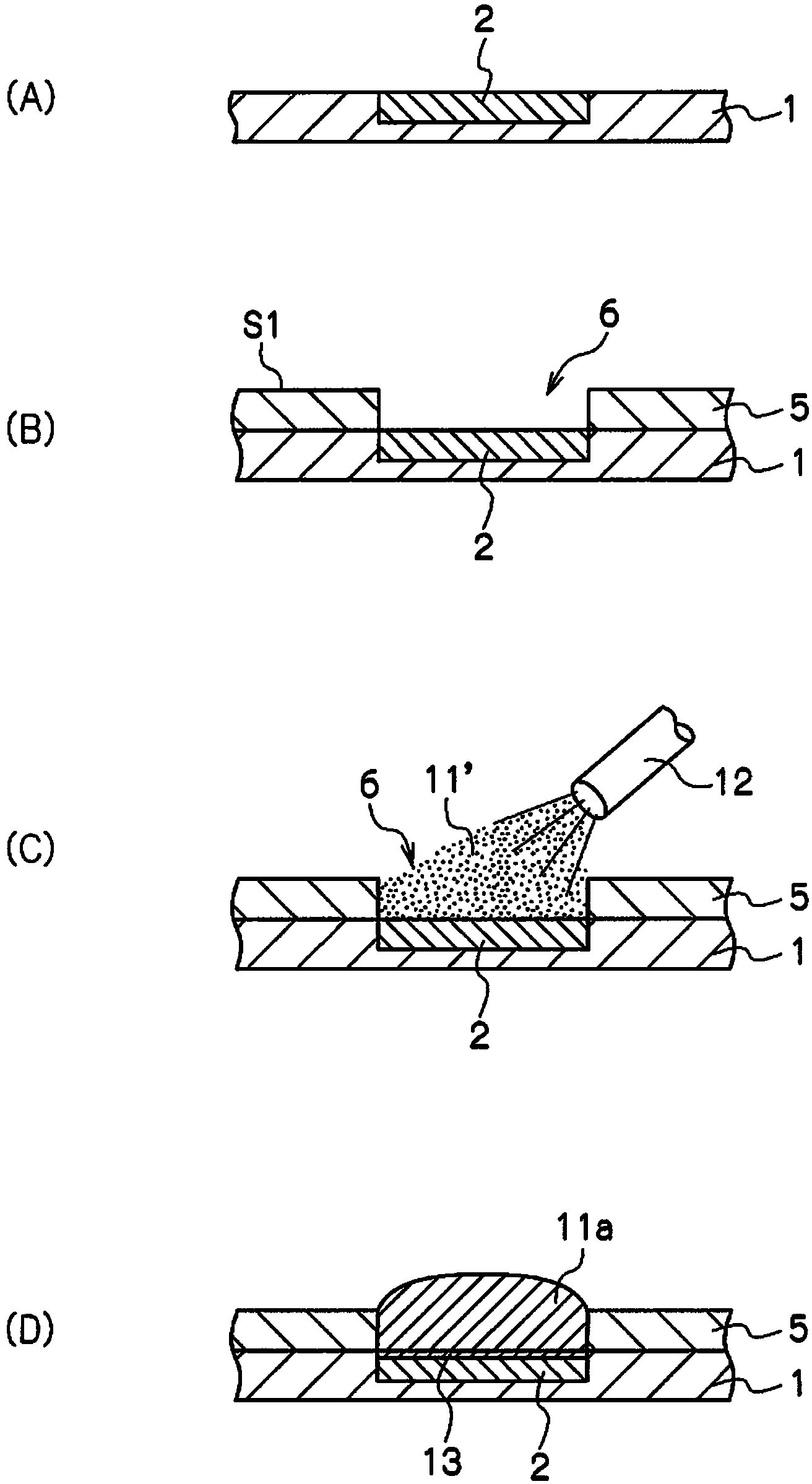
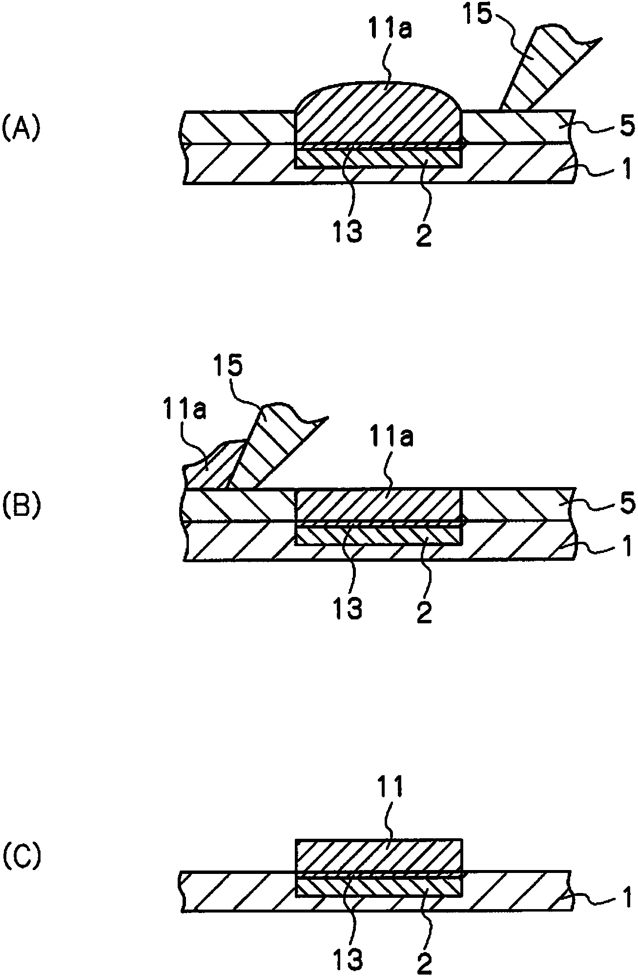
[0113]As an example, a substrate 1 on which a copper wiring pattern having a width of, for example, 200 μm and a thickness of, for example, 10 μm is formed is prepared. In the substrate 1 , only the connecting portion of the copper wiring pattern with a width of, for example, 200 μm and a length of, for example, 50 μm is exposed, and the other copper electrodes 2 are covered with an insulating layer. A mask 5 having openings 6 for forming solder bumps 11 on the above-mentioned connection portions was prepared. After aligning and superimposing the connecting portion where the copper electrode 2 is exposed on the substrate 1 and the opening 6 of the mask 5, use Ni: 0.05% by mass, Ge: 0.005% by mass, Ag: 3% by mass, Cu: 0.5% by mass The quinary system lead-free solder consisting of mass % and the balance of Sn is heated to 250° C. to form molten solder 11 a , and jet 11 ′ of this molten solder is sprayed toward opening 6 . The jet flow 11' of molten solder is performed with the ...

Embodiment 2

[0117] In Example 1, as the solder material, a quinary system lead-free solder consisting of Ni: 0.03% by mass, Ge: 0.005% by mass, Ag: 3% by mass, Cu: 0.5% by mass, and Sn as the balance was used. In addition, the solder bump 11 of Example 2 was formed similarly to Example 1. As in Example 1, it can be seen from the scanning electron micrograph of the cross-section that the CuNiSn intermetallic compound layer 13 a is formed with a thickness of 1 μm although slightly uneven.

Embodiment 3

[0119] In Example 1, as the solder material, a quinary system lead-free solder consisting of Ni: 0.07% by mass, Ge: 0.005% by mass, Ag: 3% by mass, Cu: 0.5% by mass, and Sn as the balance was used. In addition, the solder bump 11 of Example 3 was formed similarly to Example 1. FIG. As in Example 1, it can be seen from the scanning electron micrograph of the cross section that the CuNiSn intermetallic compound layer 13 a is uniformly formed with a thickness of 2 μm.


PUM

PropertyMeasurementUnit
thicknessaaaaaaaaaa
thicknessaaaaaaaaaa
thicknessaaaaaaaaaa

Abstract

The invention provides a solder bump forming method capable of forming solder bumps having a desired constant thickness, without any failure such as copper corrosion, on a mounting board such as a printed circuit board having fine copper electrodes. The solder bump forming method includes: a process in which a prepared mask (5) is placed on a prepared substrate (1) and then a molten solder jet is blown to fill an opening of the mask (5) with molten solder (11a) until the molten solder (11a) exceeds the thickness of the mask (5); a process of removing a part of the molten solder (11a) that exceeds the thickness of the mask (5) to form a solder bump (11) having a predetermined thickness; and a process of removing the mask (5). The molten solder (11a) is molten lead-free solder that includes tin as a main ingredient and at least nickel as a sub ingredient, and further includes one or more other ingredients such as silver, copper, and germanium. The part of the molten solder (11a) that exceeds the thickness of the mask (5) is removed by using a blade or an air cutter or by spraying a solution (18) that includes organic fatty acid having 12 to 20 carbon atoms.

Description

technical field [0001] The present invention relates to a solder bump, a method for forming the same, a substrate provided with the solder bump, and a method for manufacturing the same. More specifically, it relates to a solder bump having a certain thickness on a copper electrode provided on a substrate such as a printed circuit board, a wafer, and a flexible substrate, which can prevent corrosion of copper constituting the copper electrode, a method for forming the same, and a solder bump having such a solder bump. Block substrate and manufacturing method thereof. Background technique [0002] In recent years, the wiring density and mounting density of substrates such as printed circuit boards, chips, and flexible substrates (hereinafter, these may be referred to as "mounting substrates") have been increasing. As solder bumps for soldering electronic components to mounting substrates, they are required to be fine and uniform in shape, size, and the like. As a method of f...

Claims


Application Information

Patent Timeline
Patent Type & Authority Applications(China)
IPC IPC(8): H01L21/60
CPCH01L21/4853H01L23/49811H01L24/05H01L24/11H01L24/13H01L2224/11849H01L2224/13118H01L2224/1312H01L2224/13139H01L2224/13111H01L2224/13113H01L2224/131H01L2224/1181H01L2224/11821H01L2224/11472H01L2224/11312H01L2224/05647H01L2224/05571H01L2224/05147H01L2224/05026H01L2224/0401H01L2224/16503H01L2224/13155H01L2224/94H01L2924/00014H01L2924/00012H01L2924/01028H01L2924/0105H01L2924/01047H01L2924/01029H01L2924/014H01L2924/0132H01L2224/11H01L2224/05552H05K3/282H05K3/3468H05K2203/0557H05K2203/0746H05K2203/1344B23K37/06H05K13/0465
Inventor 谷黑克守
Owner TANIGUROGUMI CORP
Why Eureka
Try Eureka