

Method for manufacturing selective emitter solar cell
A solar cell and emitter technology, applied in the field of solar cells, can solve the problems of secondary pollution, cell pollution, low cell processing efficiency, etc., and achieve the effects of easy cleaning, improving efficiency, and realizing large-scale industrial production.
- Summary
- Abstract
- Description
- Claims
- Application Information
AI Technical Summary
Problems solved by technology
Method used
Image

Examples
Embodiment 1
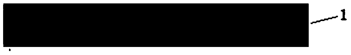
[0043] 1. Such as figure 1 As shown, a P-type silicon wafer 1 with good performance, high purity, and resistivity of 10 ohm / cm is taken and subjected to KOH alkaline polishing to remove scratches and uneven areas on the surface of the bare silicon wafer.
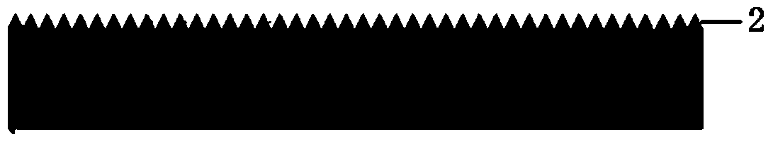
[0044] 2. Such as figure 2 As shown, the silicon wafer is reacted in an alkaline solution to form an inverted pyramid texture structure 2, and then acid cleaning is performed to remove the scratch damage layer, organic matter and metal ions on the surface of the silicon wafer.
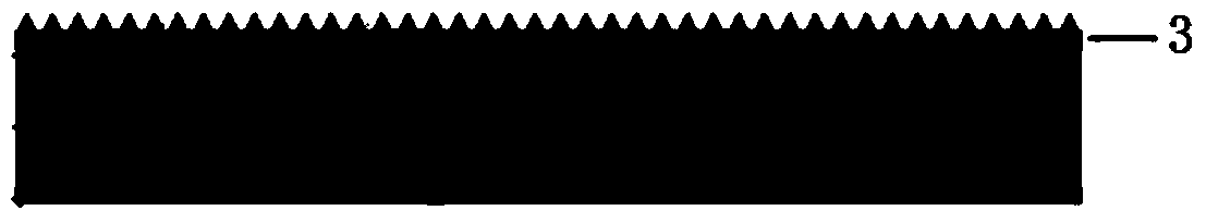
[0045] 3. Such as image 3 As shown, put the silicon wafer into a diffusion furnace for diffusion, using liquid POCl 3 As a diffusion source, diffusion is performed at 850°C to form n on the surface 3 of the silicon wafer. + Layer, square resistance is 20ohm / sq, after diffusion, use hydrofluoric acid to remove surface phosphorous silicate glass.
[0046] 4. Such as Figure 4 As shown, the screen printing barrier ink paste 4RSTINK SCR CLEAR (purchased from ...
Embodiment 2
[0053] 1. Such as figure 1 As shown, a P-type silicon wafer 1 with good performance, high purity, and resistivity of 3 ohm / cm is taken and subjected to KOH alkaline polishing to remove scratches and uneven areas on the surface of the bare silicon wafer.
[0054] 2. Such as figure 2 As shown, the silicon wafer is reacted in an alkaline solution to form an inverted pyramid texture structure 2, and then acid cleaning is performed to remove the scratch damage layer, organic matter and metal ions on the surface of the silicon wafer.
[0055] 3. Such as image 3 As shown, put the silicon wafer into a diffusion furnace for diffusion, using liquid POCl 3 As a diffusion source, diffusion is performed at 850°C to form n on the surface 3 of the silicon wafer. + Layer, square resistance is 20ohm / sq, after diffusion, use hydrofluoric acid to remove surface phosphorous silicate glass.
[0056] 4. Such as Figure 4 As shown, the screen printing barrier ink paste 4 Resist Ink (purchased from PVGS c...
Embodiment 3
[0063] 1. Such as figure 1 As shown, a P-type silicon wafer 1 with good performance, high purity, and resistivity of 5 ohm / cm is taken and subjected to KOH alkaline polishing to remove scratches and uneven areas on the surface of the bare silicon wafer.
[0064] 2. Such as figure 2 As shown, the silicon wafer is reacted in an alkaline solution to form an inverted pyramid texture structure 2, and then acid cleaning is performed to remove the scratch damage layer, organic matter and metal ions on the surface of the silicon wafer.
[0065] 3. Such as image 3 As shown, put the silicon wafer into a diffusion furnace for diffusion, using liquid POCl 3 As a diffusion source, diffusion is performed at 850°C to form n on the surface 3 of the silicon wafer. + Layer, square resistance is 20ohm / sq, after diffusion, use hydrofluoric acid to remove surface phosphorous silicate glass.
[0066] 4. Such as Figure 4 As shown, the screen printing barrier ink paste 4 Resist Ink (purchased from PVGS c...
PUM
| Property | Measurement | Unit |
|---|---|---|
| Sheet resistance | aaaaa | aaaaa |
| Thickness | aaaaa | aaaaa |
Abstract
Description
Claims
Application Information