Tool for measuring surface evenness of wafer

A surface flatness and chip technology, applied in the field of LED chip production process equipment, can solve the problems of long measurement time, low measurement efficiency, pollution, etc., and achieve the effects of fast measurement speed, simple structure and high measurement accuracy

Inactive Publication Date: 2015-01-14
TIANJIN HAOYANG HUANYU TECH
View PDF0 Cites 9 Cited by
  • Summary
  • Abstract
  • Description
  • Claims
  • Application Information

AI Technical Summary

Problems solved by technology

The thickness of the sapphire wafer after processing needs to be accurate to the micron level. The measurement of the wafer is carried out on a marble plane. The traditional wafer flatness measurement technology cannot accurately measure the surface flatness due to the warping of the wafer to varying degrees and manual pressure measurement. The error range is large; the damage to the wafer during the pressing process is large, and it is easy to cause scratches, crushing, edge knocking, pollution and other undesirable phenomena; and the long measurement time results in poor efficiency and low measurement efficiency

Method used


Image

  • Tool for measuring surface evenness of wafer
  • Tool for measuring surface evenness of wafer

Examples


Embodiment Construction

[0010] In order to enable those skilled in the art to better understand the technical solutions of the present invention, the present invention will be further described in detail below in conjunction with the accompanying drawings and embodiments.

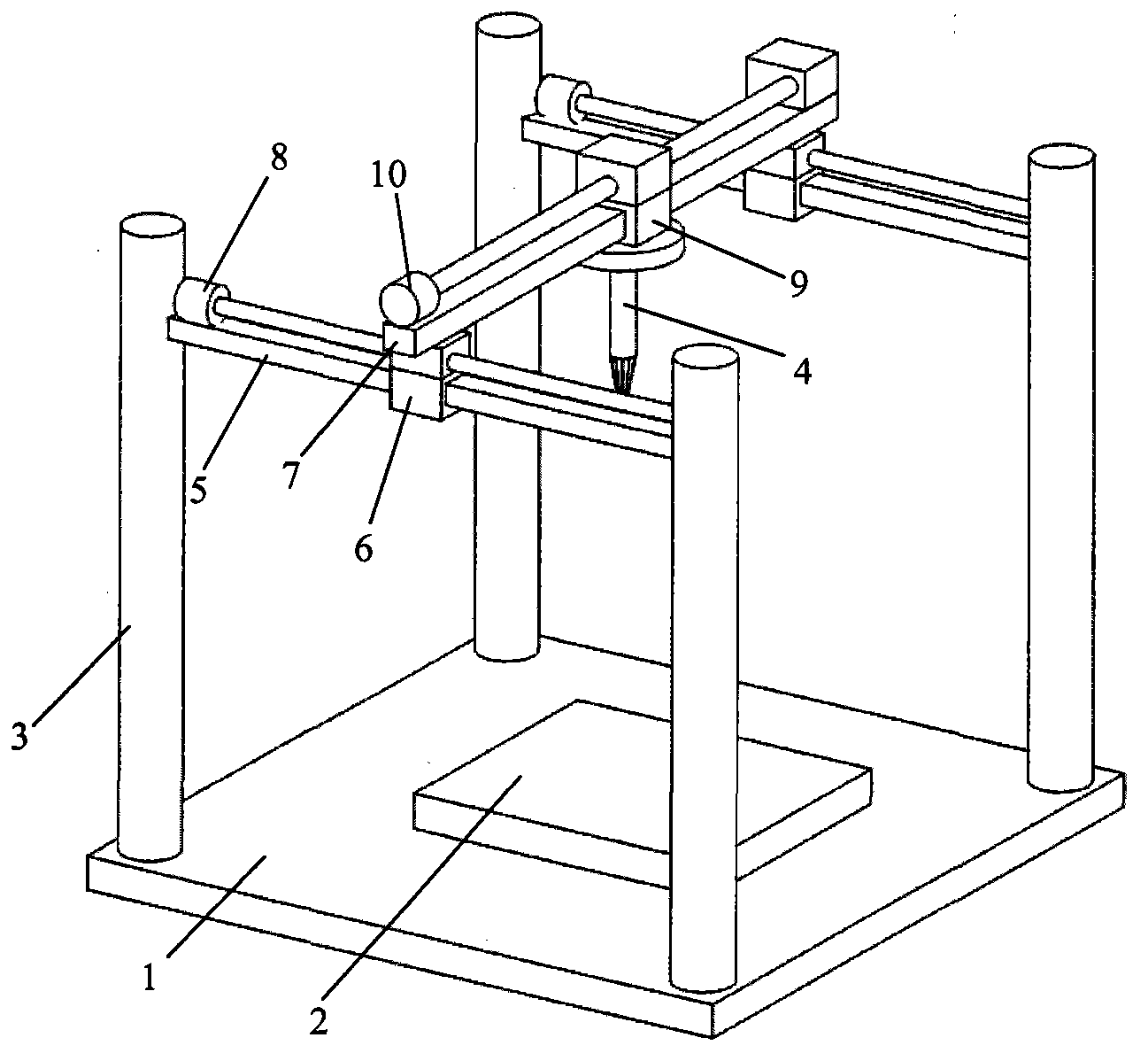
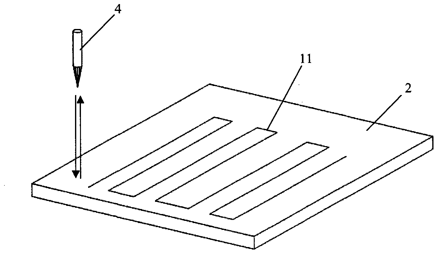
[0011] Such as figure 1 , 2 As shown, the tooling used for wafer surface flatness measurement of the present invention comprises a base 1 arranged horizontally, on which a wafer placement area is arranged, and a wafer 2 is placed in this area to be inspected; the support 3 is located on the base 1, and the support 3 is provided with a laser range finder 4 and an X-axis translation mechanism and a Y-axis translation mechanism for driving the laser range finder to move, and the laser range finder 4 is vertically arranged.

[0012] The X-axis translation mechanism includes an X-axis guide rail 5 arranged along the X-axis direction and an X-axis slider 6 located on the X-axis guide rail 5. A Y-axis guide rail 7 is fixed on the X-axis...


PUM


Abstract

The invention discloses a tool for measuring the surface evenness of a wafer, wherein the tool can rapidly and precisely measure the surface evenness of the wafer without scratching or crashing or hitting or contaminating the wafer. The tool comprises a horizontal base. A wafer containing area is arranged on the base. A support is located on the base. A laser range finder, an X-axis horizontally-moving mechanism for driving the laser range finder to move and a Y-axis horizontally-moving mechanism for driving the laser range finder to move are arranged on the support. The laser range finder is vertically arranged. By means of the tool for measuring the surface evenness of the wafer, through the method that measuring points of the laser range finder walk on the surface of the wafer in the use process, the distance between the laser range finder and each measuring point on the surface of the wafer is measured, and whether the surface of the wafer is even or not can be judged by comparing the measured distance values. The tool is simple in structure, can effectively overcome the defects in the prior art and ensure the completeness of the surface of the wafer, and is high in measurement accuracy and measurement speed.

Description

technical field [0001] The invention relates to LED wafer production process equipment, in particular to a tool for measuring the flatness of the wafer surface. Background technique [0002] Sapphire is an aluminum oxide single crystal material with very high hardness. It is currently a commonly used substrate material in the LED industry. It is used as a substrate for epitaxial growth such as gallium nitride to produce light-emitting diodes such as blue light. Wafer flatness measurement after substrate processing is an important link in the LED industry chain, which needs to achieve very high precision, especially for the substrate used to make patterned wafers, which requires a flatness of less than 5 microns. The existing flatness measurement process of the sapphire substrate generally measures the surface flatness by manual pressing measurement. The thickness of the sapphire wafer after processing needs to be accurate to the micron level. The measurement of the wafer is...

Claims


Application Information

Patent Timeline
Patent Type & Authority Applications(China)
IPC IPC(8): H01L21/66
CPCG01B11/30H01L22/12
Inventor 沙恩水
Owner TIANJIN HAOYANG HUANYU TECH
Why Eureka
Try Eureka