

A kind of pcb surface treatment method
A surface treatment and concentration technology, applied in the secondary treatment of printed circuits, the formation of electrical connection of printed components, electrical components, etc., can solve the problems of contaminated gold surface, long process flow, unclean development, etc. The effect of reducing process flow and maintaining solderability
- Summary
- Abstract
- Description
- Claims
- Application Information
AI Technical Summary
Problems solved by technology
Method used
Image

Examples
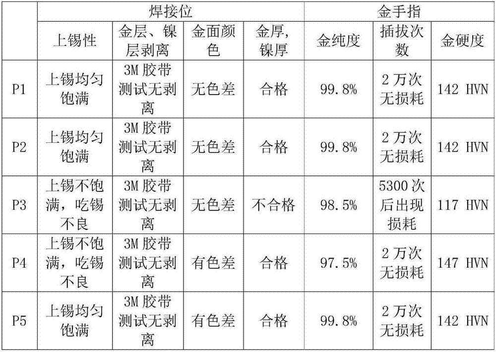
Embodiment 1
[0018] A PCB surface treatment method provided in this embodiment includes two surface treatments of immersion nickel gold and electric gold finger, and the method specifically includes the following steps:
[0019] (1) According to the existing PCB production technology, the board is first cut, and then each PCB production unit (PNL) is sequentially subjected to wet film coating, exposure, development, etching and film removal, so as to make each inner layer board. The inner layer boards are pressed together to form a multi-layer board, and then the outer layer circuits are made on the multi-layer board to form a PCB semi-finished board. details as follows:
[0020] Cutting: Cut out the core board according to the board size 520mm*620mm, and the thickness of the core board is 0.5mm H / H.
[0021] Inner layer: Produced by a vertical coating machine, the film thickness is controlled to 8μm, and a fully automatic exposure machine is used to complete the inner layer circuit expos...
Embodiment 2
[0045] This embodiment provides a PCB surface treatment method, which includes two surface treatments of immersion nickel gold and electric gold finger. is 30°C.
[0046] The resulting PCB is labeled P2.
PUM
 Abstract
Description
Claims
Application Information