Light-emitting diode and manufacturing method thereof

A technology of light-emitting diodes and electrodes, applied in electrical components, circuits, semiconductor devices, etc., can solve the problems of high cost and large consumption of gold, and achieve the effect of reducing costs and reducing gold consumption

Inactive Publication Date: 2015-01-28
HC SEMITEK SUZHOU
View PDF5 Cites 10 Cited by
  • Summary
  • Abstract
  • Description
  • Claims
  • Application Information

AI Technical Summary

Problems solved by technology

[0005] Most of the metal in the traditional red-yellow quaternary light-emitting diode chip is made of gold Au, and the gold consumption in the chip manufacturing process is very large, resulting in high cost

Method used


Image

  • Light-emitting diode and manufacturing method thereof
  • Light-emitting diode and manufacturing method thereof
  • Light-emitting diode and manufacturing method thereof

Examples


Embodiment 1

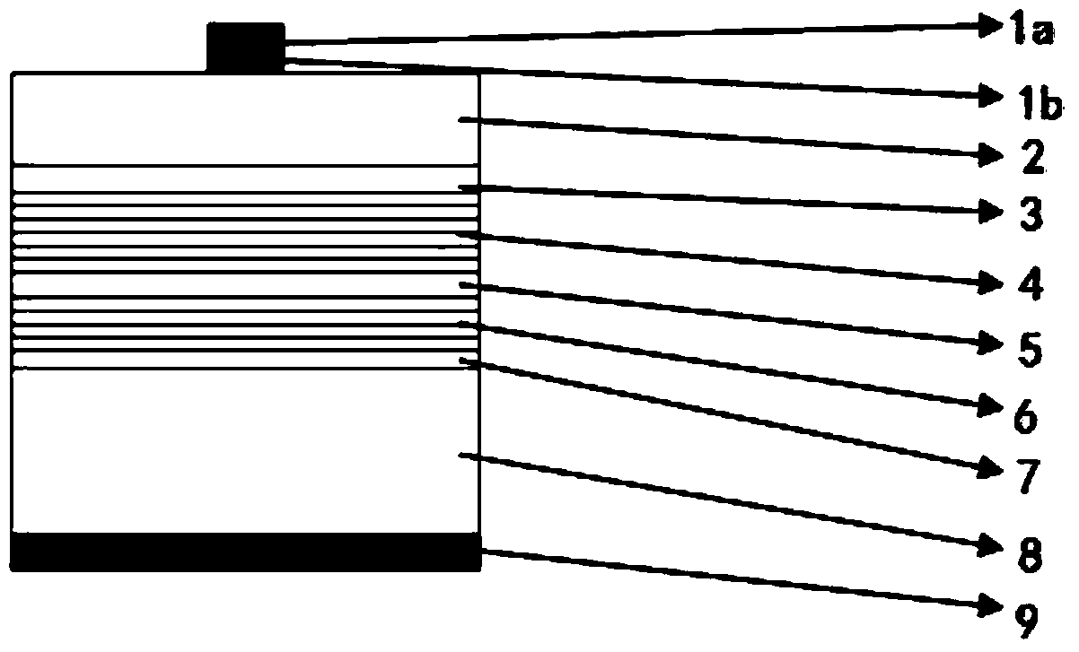
[0040] see figure 2 , an embodiment of the present invention provides a light emitting diode, including a substrate 11, a buffer layer 12, a distributed Bragg reflector 13, an n-type confinement layer 14, an active layer 15, a p-type confinement layer 16, and a GaP window layer stacked in sequence 17. P-type ohmic contact layer 18, an n-type ohmic contact electrode 10 is provided on the side of the substrate 11 opposite to the buffer layer 12, and a p-surface is provided on the side of the p-type ohmic contact layer 18 opposite to the GaP window layer 17 The bonding wire electrode 19, the C element heavily doped GaP layer 20 is laminated between the GaP window layer 17 and the p-type ohmic contact layer 18, the p-type ohmic contact layer 18 is an indium tin oxide film, and the p-side bonding wire electrode 19 is an Al electrode .

[0041] Specifically, in this embodiment, the substrate 11 can be a GaAs substrate, the buffer layer 12 can be GaAs, the distributed Bragg mirror ...

Embodiment 2

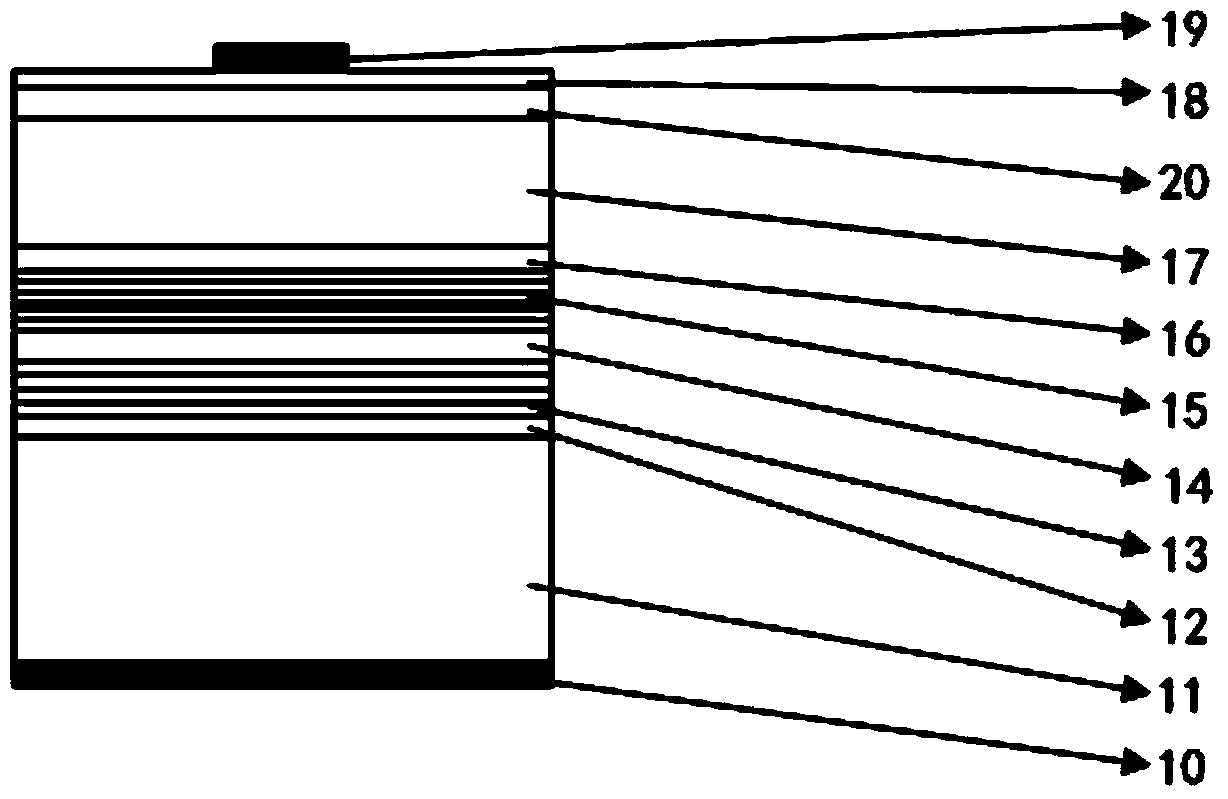
[0052] see Figure 5 , the embodiment of the present invention provides a method for manufacturing a light-emitting diode, which can be used to prepare the light-emitting diode (especially the red and yellow light-emitting diode) provided in Example 1. The method includes:

[0053] S10: providing a substrate;

[0054] In this embodiment, the substrate of the light emitting diode is a GaAs substrate.

[0055] S11: sequentially forming a buffer layer, a distributed Bragg reflector, an n-type confinement layer, an active layer, a p-type confinement layer, a GaP window layer, and a surface C heavily doped layer on the substrate;

[0056] Among them, the doping concentration of C element is greater than 1x10 19 cm -3 , the C element heavily doped the GaP layer 20 to a degree of 400-1000nm.

[0057] S12: Evaporate a layer of indium tin oxide film on the C element heavily doped GaP layer to form a p-type ohmic contact layer;

[0058] In this embodiment, an electron beam is used ...

Embodiment 3

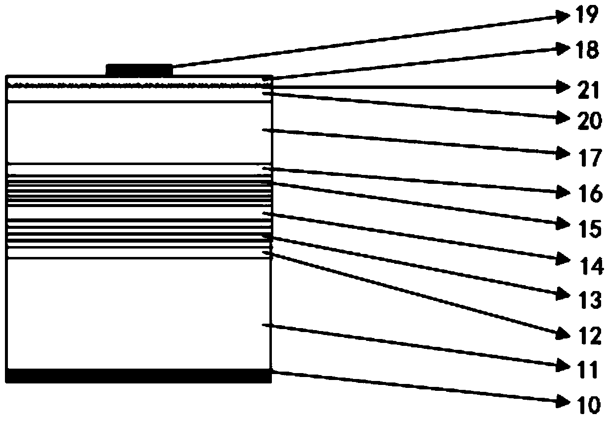
[0069] see Figure 6 , the embodiment of the present invention provides a method for manufacturing a light-emitting diode, which can be used to prepare the light-emitting diode (especially the red and yellow light-emitting diode) provided in Example 1. The difference from the method for manufacturing the diode in Example 2 is that A surface roughening layer is formed, the method comprising:

[0070] S20: providing a substrate;

[0071] In this embodiment, the substrate of the light emitting diode is a GaAs substrate.

[0072] S21: sequentially forming a buffer layer, a distributed Bragg reflector, an n-type confinement layer, an active layer, a p-type confinement layer, a GaP window layer, and a surface C heavily doped layer on the substrate;

[0073] Among them, the doping concentration of C element is greater than 1x10 19 cm -3 , the C element heavily doped the GaP layer 20 to a degree of 400-1000nm.

[0074] S22: performing surface roughening on the C element heavily d...


PUM


Abstract

The invention discloses a light-emitting diode, and belongs to the technical field of photoelectron manufacturing. The light-emitting diode comprises a substrate, a buffer layer, a distribution Prague reflection mirror, an n type limiting layer, an active layer, a p type limiting layer, a GaP window layer and a p type ohmic contact layer which are overlapped in sequence. An n type ohmic contact electrode is arranged on the face, opposite to the buffer layer, of the substrate. A p face bonding wire electrode is arranged on the face, opposite to the GaP window layer, of the p type ohmic contact layer. C element heavily-doped GaP layers overlap between the GaP window layer and the p type ohmic contact layer. The p type ohmic contact layer is an indium tin oxide film. The p face bonding wire electrode is an Al electrode. The p type ohmic contact layer is made of high-transmittance conducting film indium tin oxide instead of Au / AuBe / Au, the electrode mainly made of metal AL is adopted as the p face bonding wire electrode, and therefore the gold consumption in the chip manufacturing process can be greatly lowered, and cost can be effectively and greatly reduced.

Description

technical field [0001] The invention relates to the field of optoelectronic manufacturing technology, in particular to a light emitting diode and a manufacturing method thereof. Background technique [0002] As a new lighting technology, LED uses semiconductor chips as light-emitting materials to directly convert electrical energy into light energy. Semiconductor LEDs and their applications are considered to be one of the most promising high-tech fields in the 21st century due to their advantages such as high luminous efficiency, low power consumption, long service life, strong safety and reliability, environmental protection and sanitation. At present, about 70% of the manufacturing cost of LED chips comes from precious metals, especially the cost of gold Au materials. How to gain a firm foothold in the crazy price war, cost reduction is an important factor. [0003] At present, the traditional red-yellow quaternary light-emitting diode chip structure includes a p-side bon...

Claims


Application Information

Patent Timeline
Patent Type & Authority Applications(China)
IPC IPC(8): H01L33/38H01L33/42H01L33/00
CPCH01L33/38H01L33/005H01L33/305H01L33/42H01L2933/0008H01L2933/0016
Inventor 薛蕾肖千宇
Owner HC SEMITEK SUZHOU
Why Eureka
Try Eureka