Perovskite type solar cell with sputtering ZnO as electron transfer layer and preparation
An electron transport layer and solar cell technology, applied in the field of solar cells, can solve problems such as complex processes, and achieve the effects of high electron transport capacity, high photoelectric conversion efficiency, and easy fabrication
- Summary
- Abstract
- Description
- Claims
- Application Information
AI Technical Summary
Problems solved by technology
Method used
Image
Examples
Embodiment 1
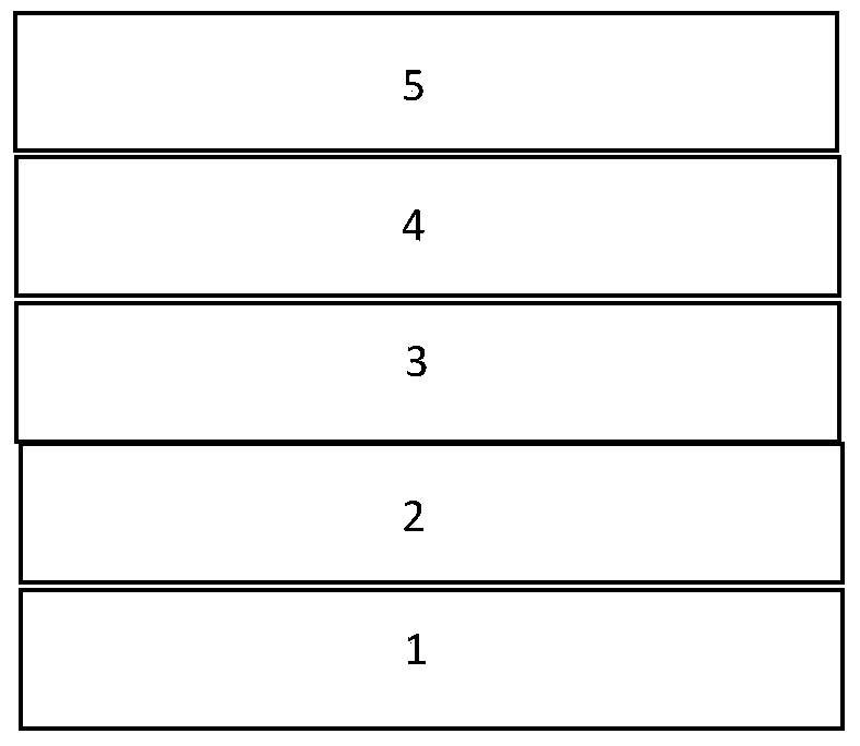
[0033] A perovskite type solar cell with sputtered ZnO as the electron transport layer, such as figure 1 As shown, it is composed of a transparent conductive glass substrate 1, an electron transport layer 2, a perovskite-type material layer 3, a hole transport layer 4 and an Au / Ag metal back electrode layer 5 and constitutes a laminated structure in sequence. The transparent conductive The glass substrate 1 is ITO conductive glass; the electron transport layer 2 is a sputtered ZnO film with a thickness of 40 nm; the perovskite material layer 3 is CH 3 NH 3 PbI 3 Layer with a thickness of 300nm; hole transport layer 4 is 2,2',7,7'-tetra[N,N-bis(4-methoxyphenyl)amino]-9,9'-spirobifluorene ( The spiro-MeOTAD) layer has a thickness of 40 nm; the metal back electrode layer 5 is Ag with a thickness of 100 nm.
Embodiment 2
[0035] A perovskite type solar cell with sputtered ZnO as the electron transport layer, which is composed of a transparent conductive glass substrate, an electron transport layer, a perovskite type material layer, a hole transport layer and an Au / Ag metal back electrode layer. The laminated structure is formed in sequence, the transparent conductive glass substrate is ITO conductive glass; the electron transport layer is a sputtered ZnO film with a thickness of 20nm; the perovskite-type material layer is CH 3 NH 3 PbI 3 Layer with a thickness of 300nm; the hole transport layer is 2,2',7,7'-tetra[N,N-bis(4-methoxyphenyl)amino]-9,9'-spirobifluorene (spiro -MeOTAD) layer with a thickness of 40nm; the metal back electrode layer is Ag with a thickness of 60nm.
Embodiment 3
[0037] A perovskite type solar cell with sputtered ZnO as the electron transport layer, which is composed of a transparent conductive glass substrate, an electron transport layer, a perovskite type material layer, a hole transport layer and an Au / Ag metal back electrode layer. The laminated structure is formed in sequence, the transparent conductive glass substrate is ITO conductive glass; the electron transport layer is a sputtered ZnO film with a thickness of 120 nm; the perovskite-type material layer is CH 3 NH 3 PbI 3 Layer with a thickness of 300nm; the hole transport layer is 2,2',7,7'-tetra[N,N-bis(4-methoxyphenyl)amino]-9,9'-spirobifluorene (spiro -MeOTAD) layer with a thickness of 40nm; the metal back electrode layer is Au with a thickness of 60nm.
PUM
 Abstract
Description
Claims
Application Information
