
Method for arranging multiple layers of electronic elements on single-surface stereo circuit and device prepared by the same

A technology of three-dimensional circuits and electronic components, applied in electrical components, printed circuit manufacturing, printed circuits, etc., can solve the problems of inability to place parts and small internal space, and achieve the effect of saving internal space, saving resources and reducing costs

Inactive Publication Date: 2015-01-28
COSONIC INTELLIGENT TECH CO LTD
View PDF4 Cites 2 Cited by
  • Summary
  • Abstract
  • Description
  • Claims
  • Application Information

AI Technical Summary

Problems solved by technology

The continuous miniaturization of some portable mobile electronic products makes the internal space smaller and smaller, and the package of components is also made smaller again and again, and it is impossible to place the required parts in the effective circuit board space.

Method used


Image

  • Method for arranging multiple layers of electronic elements on single-surface stereo circuit and device prepared by the same
  • Method for arranging multiple layers of electronic elements on single-surface stereo circuit and device prepared by the same
  • Method for arranging multiple layers of electronic elements on single-surface stereo circuit and device prepared by the same

Examples


Embodiment 1

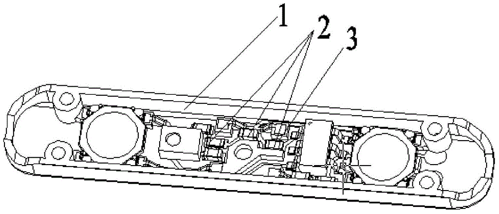
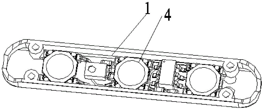
[0030] A method for placing multilayer electronic components on a single-sided three-dimensional circuit, comprising the following steps:

[0031] 1) Firstly, a pit for assembling small packaged electronic components is formed on the plastic structural part;

[0032] 2) Then, absorb a layer of copper powder on the plastic structure with pits obtained in step 1;

[0033] 3) Place the plastic structural parts that have absorbed the copper powder in step 2 in a nitrogen atmosphere, and then a laser machine loaded with a designed circuit pattern selectively scans the copper powder, and the scanned copper powder instantly melts and combines with the plastic The structural parts are welded together to form a three-dimensional circuit, and then the machine vibrates to shake off the unscanned copper powder;

[0034] 4) Finally, assemble small packaged electronic components on the three-dimensional circuit in the pit of the plastic structural part, and assemble large packaged electron...

Embodiment 2

[0041] A method for placing multilayer electronic components on a single-sided three-dimensional circuit, comprising the following steps:

[0042] 1) Firstly, a pit for assembling small packaged electronic components is formed on the plastic structural part;

[0043] 2) Then spray one layer of aluminum powder on the plastic structural part with pits obtained in step 1;

[0044] 3) Place the plastic structural parts sprayed with aluminum powder in step 2 in an argon atmosphere, and then a laser machine loaded with a designed circuit pattern selectively scans the aluminum powder, and the scanned aluminum powder instantly melts and combines with the plastic The structural parts are welded together to form a three-dimensional circuit, and then the unscanned aluminum powder is removed with a brush;

[0045] 4) Finally, assemble small packaged electronic components on the three-dimensional circuit in the pit of the plastic structural part, and assemble large packaged electronic com...

Embodiment 3

[0051] A method for placing multilayer electronic components on a single-sided three-dimensional circuit, comprising the following steps:

[0052] 1) Firstly, a pit for assembling small packaged electronic components is formed on the plastic structural part;

[0053] 2) then spread a layer of nickel powder on the plastic structural part with pits obtained in step 1;

[0054] 3) Place the plastic structural parts covered with nickel powder in step 2 in a carbon dioxide atmosphere, and then selectively scan the nickel powder with a laser machine loaded with a designed circuit pattern. The scanned nickel powder melts instantly, and the plastic structure The pieces are welded together to form a three-dimensional circuit, and then the unscanned nickel powder is removed with a brush;

[0055] 4) Finally, assemble small packaged electronic components on the three-dimensional circuit in the pit of the plastic structural part, and assemble large packaged electronic components on the t...


PUM

PropertyMeasurementUnit
Wavelengthaaaaaaaaaa

Abstract

The invention relates to the technical field of stereo circuits and devices, in particular to a method for arranging multiple layers of electronic elements on a single-surface stereo circuit and a device prepared by the same. Compared with the prior art, the method for arranging multiple layers of electronic elements on the single-surface stereo circuit includes steps that 1) forming pits for assembling small encapsulated electronic components in a plastic-rubber structure piece; 2) flatly paving, adsorbing or coating one layer of conductive powder on the plastic-rubber structure piece with the pits of the step 1); 3) arranging the plastic-rubber structure piece provided with the conductive powder in the flat paving, adsorbing or coating mode of the step 2 in a gas atmosphere, using a laser machine loaded with designed circuit patterns to selectively scan the conductive powder, wherein the scanned conductive powder is fused instantaneously to weld with the plastic-rubber structure piece to form the stereo circuit; removing the conductive powder which is not scanned; 4) assembling large and small elements and components. The method for arranging multiple layers of electronic elements on the single-surface stereo circuit saves the inside space for an electronic product and lowers the cost; the method for arranging multiple layers of electronic elements on the single-surface stereo circuit can prepare Bluetooth earphones, Bluetooth box bodies, headset wire controllers, Bluetooth bracelets or the same, and the application is broad.

Description

technical field [0001] The invention relates to the technical field of three-dimensional circuits and devices, in particular to a method for placing multilayer electronic components on a single-sided three-dimensional circuit and a device for preparing the same. Background technique [0002] At present, the structure of the circuit board is flat, and the electronic components are placed on the circuit board in a single layer. Only when there is a space on the side of the circuit board where the large package parts are attached, can the components be overlapped; the existing circuit boards are all It uses flat plates such as glass fiber and cardboard as circuit supports to form circuits on the plane. These support materials will occupy the physical space of the product, and these support materials are also non-recyclable electronic waste in the world. The continuous miniaturization of some portable mobile electronic products makes the internal space smaller and smaller, and t...

Claims


Application Information

Patent Timeline
IPC IPC(8): H05K3/30H05K3/02
CPCH05K3/30H05K3/301H05K2203/13
Inventor 胡平
Owner COSONIC INTELLIGENT TECH CO LTD
Learn More