Method for improving negative bias temperature stability of grid of PMOS device

A technology of negative bias temperature and stability, which is applied in semiconductor devices, semiconductor/solid-state device manufacturing, electrical components, etc. shift and other issues, to solve the problem of negative bias temperature instability, improve the stability of negative bias temperature, and reduce the effect of threshold voltage drift

Active Publication Date: 2015-02-11
SHANGHAI HUAHONG GRACE SEMICON MFG CORP
View PDF4 Cites 5 Cited by
  • Summary
  • Abstract
  • Description
  • Claims
  • Application Information

AI Technical Summary

Problems solved by technology

Although the above method can suppress the depletion of gate polysilicon, the newly introduced titanium is easily oxidized and expanded in the subsequent gate polysilicon re-oxidation (Re-oxidation) process, resulting in spherical protrusions (pilling), which It will greatly affect the morphology of the gate structure, which is not conducive to the stability of the device performance
At the same time, the introduction of titanium also poses a risk of metal ion contamination to products on the process line
[0005] In addition, if figure 1 or 2, in the existing process technology, after the pattern etching of the gate polysilicon 103 is completed, the silicon or silicon oxide interface such as the silicon substrate 101 and the gate oxide layer 102 interface, the gate polysilicon 103 and the gate oxide layer 102 interface, and the silicon-hydrogen bond (Si-H bond) is formed at the interface of the gate silicon nitride layer 106, and hydrogen is easy to diffuse at the interface, resulting in a large number of interface states, so that under the action of pressure or high temperature, it is easier to make silicon The breaking of hydrogen bonds and the diffusion of hydrogen cause the threshold voltage of PMOS to shift greatly and the saturation leakage current increases, which will cause the problem of negative bias temperature independency (NBTI)

Method used


Image

  • Method for improving negative bias temperature stability of grid of PMOS device
  • Method for improving negative bias temperature stability of grid of PMOS device
  • Method for improving negative bias temperature stability of grid of PMOS device

Examples


Embodiment Construction

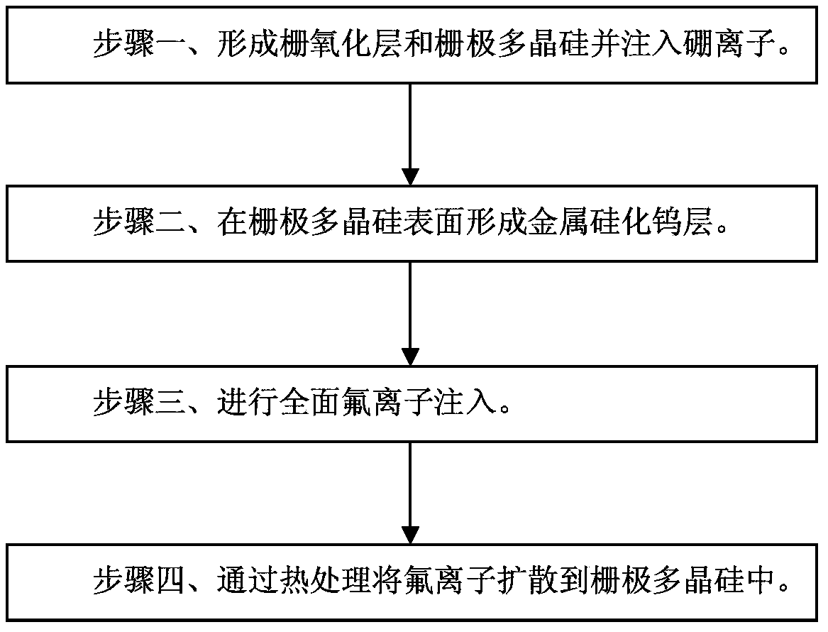
[0024] Such as image 3 Shown is the flow chart of the method of the embodiment of the present invention; the step of forming the gate of the PMOS device in the method for improving the negative bias temperature stability of the gate of the PMOS device in the embodiment of the present invention includes:

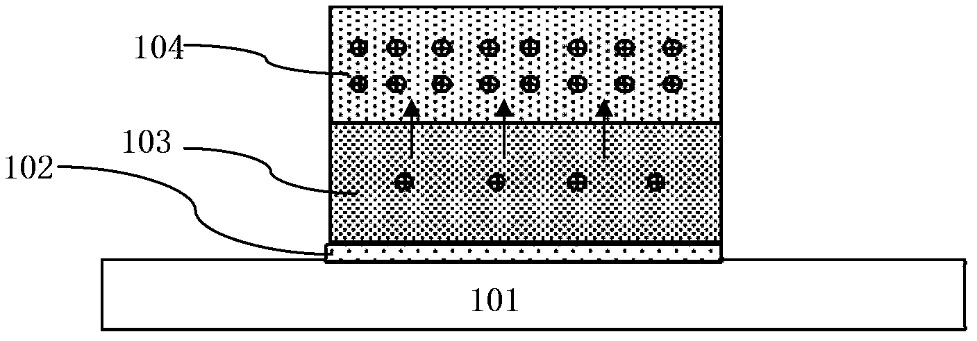
[0025] Step 1, such as Figure 4A As shown, a gate oxide layer 2 and a gate polysilicon 3 are sequentially formed on a silicon substrate 1, and boron ions are implanted into the gate polysilicon 3 in the PMOS device formation region. 1E15cm -2 ~1E16cm -2 , making the gate polysilicon 3 in the region where the PMOS device is formed have a P-type doped structure.

[0026] Step two, such as Figure 4A As shown, after boron ion implantation, a metal tungsten silicide layer 4 is formed on the surface of the gate polysilicon 3 .

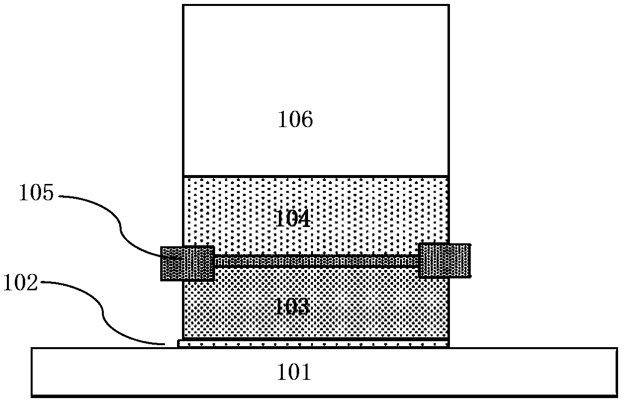
[0027] Step three, such as Figure 4B As shown, fluorine ion implantation is performed to implant fluorine ions into the metal tungsten silicide l...


PUM


Abstract

The invention discloses a method for improving the negative bias temperature stability of the grid of a PMOS device. The method comprises the following steps: forming a grid oxide layer and grid polysilicon, and injecting boron ions; forming a metal tungsten silicide layer on the surface of the grid polysilicon; performing comprehensive fluorinion injection; and diffusing fluorinions into the grid polysilicon through thermal treatment. According to the invention, the stress at the interface of silicon and silicon oxide of the grid can be decreased, the interface state generated due to the existence of hydrogen bonds is reduced, the stability of the interface of the silicon and the silicon oxide can be enhanced, the threshold voltage drift of the PMOS device can be effectively reduced, and the negative bias temperature stability of the grid of the PMOS device is improved.

Description

technical field [0001] The invention relates to a semiconductor integrated circuit manufacturing process method, in particular to a method for improving the negative bias temperature stability of a gate of a PMOS device. Background technique [0002] In the existing process, in order to facilitate the integration of NMOS devices, the gate polysilicon of PMOS devices adopts the same doping conditions as the gate polysilicon of NMOS devices, that is, both are N-type doped and require heavy doping, and the gate polysilicon of PMOS devices After N-type doping of extremely polysilicon, a P-type buried channel (buried channel) must be formed in the channel region to solve the problem of high threshold voltage (Vt) caused by N-type gate polysilicon, and the introduction of P-type buried channel will cause A large leakage current problem occurs. In order to solve the problems of higher Vt and larger leakage current caused by the buried channel of the existing PMOS device, P-type bo...

Claims


Application Information

Patent Timeline
Patent Type & Authority Applications(China)
IPC IPC(8): H01L21/28H01L21/336
CPCH01L21/28061H01L21/76895
Inventor 陈瑜马斌陈华伦罗啸郭振强
Owner SHANGHAI HUAHONG GRACE SEMICON MFG CORP
Why Eureka
Try Eureka